|
数据搜索系统,热门电子元器件搜索 |
|
|
数据搜索系统,热门电子元器件搜索 |
|
LP2996AMR/NOPB 数据表(PDF) 19 Page - Texas Instruments |
|
|
|
|||||||||||||||||||||||||||||
LP2996AMR/NOPB 数据表(HTML) 19 Page - Texas Instruments |
|
|
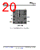
19 / 29 page  LP2996A www.ti.com SNOSCY7 – JUNE 2014 10 Layout 10.1 Layout Guidelines 1. The input capacitor for the power rail should be placed as close as possible to the PVIN pin. 2. VSENSE should be connected to the VTT termination bus at the point where regulation is required. For motherboard applications an ideal location would be at the center of the termination bus. 3. VDDQ can be connected remotely to the VDDQ rail input at either the DIMM or the Chipset. This provides the most accurate point for creating the reference voltage. 4. For improved thermal performance excessive top side copper should be used to dissipate heat from the package. Numerous vias from the ground connection to the internal ground plane will help. Additionally these can be located underneath the package if manufacturing standards permit. 5. Care should be taken when routing the VSENSE trace to avoid noise pickup from switching I/O signals. A 0.1uF ceramic capacitor located close to the SENSE can also be used to filter any unwanted high frequency signal. This can be an issue especially if long SENSE traces are used. 6. VREF should be bypassed with a 0.01 µF or 0.1 µF ceramic capacitor for improved performance. This capacitor should be located as close as possible to the VREF pin. 10.2 Layout Examples The LP2996A layout is very similar to the LP2998/Q layout. This is because the main difference between the two IC's is the wider temperature range, -40°C to 125°C, which the LP2998/Q offers. As such, the below example shows the layout from a LP2998EVM. These layout examples can be used to evaluate the LP2996A. Figure 29. LP2998EVM SO PowerPAD Layout Example (Front) Copyright © 2014, Texas Instruments Incorporated Submit Documentation Feedback 19 Product Folder Links: LP2996A |
|
|
链接网址 |
| ALLDATASHEET是否为您带来帮助? [ DONATE ] |
关于 Alldatasheet | 广告服务 | 联系我们 | 隐私政策 | 数据表链接 | 链接交换 | 制造商名单 All Rights Reserved©Alldatasheet.com |
| Russian : Alldatasheetru.com | Korean : Alldatasheet.co.kr | Spanish : Alldatasheet.es | French : Alldatasheet.fr | Italian : Alldatasheetit.com Portuguese : Alldatasheetpt.com | Polish : Alldatasheet.pl | Vietnamese : Alldatasheet.vn Indian : Alldatasheet.in | Mexican : Alldatasheet.com.mx | British : Alldatasheet.co.uk | New Zealand : Alldatasheet.co.nz |
|
Family Site : ic2ic.com |
icmetro.com |
 Chinese ▼
 English
 Chinese
 German
 Japanese
 Russian
 Korean
 Spanish
 French
 Italian
 Portuguese
 Polish
 Vietnamese
 Indian
 Mexican
 British
 New Zealand