|
数据搜索系统,热门电子元器件搜索 |
|
|
数据搜索系统,热门电子元器件搜索 |
|
FT51AL-R 数据表(PDF) 16 Page - Future Technology Devices International Ltd. |
|
|
|||||||||||||||||||||||||||||
FT51AL-R 数据表(HTML) 16 Page - Future Technology Devices International Ltd. |
|
|
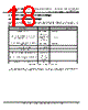
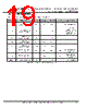
16 / 43 page  Copyright © Future Technology Devices International Limited 16 FT51A Advanced MCU with 8051 Compatible Core IC Datasheet Version 1.5 Doc ument N o.: FT _000877 C learance N o.: FT DI#420 1 stop bit 8 data bits Pull up 3.2.18 245 FIFO The 245 FIFO interface operating in asynchronous mode has an eight bit data bus, individual read and write strobes with two hardware flow control signals. 3.2.19 PWM The Pulse Width Modulation (PWM) block can generate a signal in which parameters such as period and duty cycle are controlled by the 8051 core. It provides 8 outputs and can generate a core interrupt if set. The main purpose is to generate PWM signals which can be used to control motors, DC/DC converters, AC/DC supplies, etc. 3.2.20 Digital IO pins Up to 16 General Purpose digital IO pins are available depending on the package type. 3.2.21 Analogue IO pins Up to 16 AIO pins are available depending on the package type. The pin can function in either analogue or digital mode, but not both modes at the same time . When in analogue mode all 16 AIO pins can be configured to the ADC mode. AIO_mode_1 AIO_mode_0 Configuration 0 0 Analogue off. If the pin is configured for digital mode, it can be controlled similar to digital IO pins. 0 1 Reserved. 1 0 ADC mode. Analogue input signal for the internal ADC convertor. 1 1 Reserved. Table 3-3 – AIO Modes To configure these modes, specific registers of the AIOs must be configured. On top of these modes sits a global mode which allows multiple control of AIO pins. All 16 pins can be configured depending on the package type. 3.2.22 ADC The ADC block can convert the analogue input signal to a digital value and store the value in the registers. The ADC block can be configured to work in single -ended mode and differential mode. In single-ended mode, an input signal from any of the AIO pins can be the input to the ADC block, with the reference voltage connected to VOUT3V3. In differential mode, two AIO pins are used together to form a pair of differential inputs. The voltage difference between these two pins will be converted to digital values. |
|
链接网址 |
| ALLDATASHEET是否为您带来帮助? [ DONATE ] |
关于 Alldatasheet | 广告服务 | 联系我们 | 隐私政策 | 数据表链接 | 链接交换 | 制造商名单 All Rights Reserved©Alldatasheet.com |
| Russian : Alldatasheetru.com | Korean : Alldatasheet.co.kr | Spanish : Alldatasheet.es | French : Alldatasheet.fr | Italian : Alldatasheetit.com Portuguese : Alldatasheetpt.com | Polish : Alldatasheet.pl | Vietnamese : Alldatasheet.vn Indian : Alldatasheet.in | Mexican : Alldatasheet.com.mx | British : Alldatasheet.co.uk | New Zealand : Alldatasheet.co.nz |
|
Family Site : ic2ic.com |
icmetro.com |
 Chinese ▼
 English
 Chinese
 German
 Japanese
 Russian
 Korean
 Spanish
 French
 Italian
 Portuguese
 Polish
 Vietnamese
 Indian
 Mexican
 British
 New Zealand