|
数据搜索系统,热门电子元器件搜索 |
|
|
数据搜索系统,热门电子元器件搜索 |
|
ADP7182ACPZ-R7 数据表(PDF) 24 Page - Analog Devices |
|
|
|||||||||||||||||||||||||||||
ADP7182ACPZ-R7 数据表(HTML) 24 Page - Analog Devices |
|
|
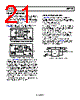
24 / 31 page  ADP7182 Data Sheet Rev. I | Page 24 of 31 NOISE REDUCTION OF THE ADJUSTABLE ADP7182 The ultralow output noise of the fixed output ADP7182 is achieved by keeping the LDO error amplifier in unity gain and setting the reference voltage equal to the output voltage. This architecture does not work for an adjustable output voltage LDO. The adjustable output ADP7182 uses the more conventional architecture where the reference voltage is fixed and the error amplifier gain is a function of the output voltage. The disadvantage of the conventional LDO architecture is that the output voltage noise is proportional to the output voltage. The adjustable LDO circuit can be modified slightly to reduce the output voltage noise to levels close to that of the fixed output of the ADP7182. The circuit shown in Figure 87 adds two additional components to the output voltage setting resistor divider. CNR and RNR are added in parallel with RFB1 to reduce the ac gain of the error amplifier. RNR is chosen to be nearly equal to RFB2; this limits the ac gain of the error amplifier to approximately 6 dB. The actual gain is the parallel combination of RNR and RFB1 divided by RFB2. This resistance ensures that the error amplifier always operates at greater than unity gain. CNR is chosen by setting the reactance of CNR equal to RFB1 − RNR at a frequency between 10 Hz and 100 Hz. This capacitance sets the frequency where the ac gain of the error amplifier is 3 dB down from the dc gain. RFB2 13kΩ RFB1 147kΩ GND EN ADJ VIN VOUT ADP7182 ON ON –2V OFF 0V 2V VIN = –16V VOUT = –15V COUT 2.2µF CNR 100nF CIN 2.2µF RNR 13kΩ Figure 87. Noise Reduction Modification to Adjustable LDO The noise of the LDO is approximately the noise of the fixed output LDO (typically 18 μV rms) times RFB2, divided by the parallel combination of RNR and RFB1. Based on the component values shown in Figure 87, the ADP7182 has the following characteristics: DC gain of 12.3 (21.8 dB) 3 dB roll-off frequency of 10.8 Hz High frequency ac gain of 1.92 (5.67 dB) Noise reduction factor of 6.41 (16.13 dB) Measured rms noise of the adjustable LDO at −200 mA without noise reduction of 220 μV rms Measured rms noise of the adjustable LDO at −200 mA with noise reduction circuit of 35 μV rms Calculated rms noise of the adjustable LDO with noise reduction (assuming 18 μV rms for fixed voltage option) of 34.5 μV rms The noise of the LDO is approximately the noise of the fixed output LDO (typically 18 μV rms) times the high frequency ac gain. The following equation shows the calculation with the values shown in Figure 87. kΩ /13 kΩ 1/147 kΩ 1/13 1 1 × μV 18 (2) Figure 88 shows the difference in noise spectral density for the adjustable ADP7182 set to −15 V with and without the noise reduction network. In the 100 Hz to 30 kHz frequency range, the reduction in noise is significant. 100k 1 10 100 1k 10k 1 100M 10M 1M 100k 10k 1k 100 10 FREQUENCY (Hz) –15V ADJ –15V ADJ NR Figure 88. −15 V Adjustable ADP7182 with and without the Noise Reduction Network (CNR and RNR) CURRENT-LIMIT AND THERMAL OVERLOAD PROTECTION The ADP7182 is protected against damage due to excessive power dissipation by current-limit and thermal overload protection circuits. The ADP7182 is designed to limit current when the output load reaches −350 mA (typical). When the output load exceeds −350 mA, the output voltage is reduced to maintain a constant current limit. Thermal overload protection is included, which limits the junction temperature to a maximum of 150°C (typical). Under extreme conditions (that is, high ambient temperature and power dissipation) when the junction temperature starts to rise above 150°C, the output is turned off, reducing the output current to 0 mA. When the junction temperature falls below 135°C, the output is turned on again, and the output current is restored to the nominal value. Consider the case where a hard short from VOUT to ground occurs. At first, the ADP7182 limits current so that only −350 mA is conducted into the short. If self-heating of the junction is great enough to cause the temperature to rise above 150°C, thermal shutdown is activated, turning off the output and reducing the output current to 0 mA. As the junction temperature cools and falls below 135°C, the output turns on and conducts −350 mA into the short, again causing the junction temperature to rise above 150°C. This thermal oscillation between 135°C and 150°C causes a current oscillation between −350 mA and 0 mA that continues as long as the short remains at the output. |
|
链接网址 |
| ALLDATASHEET是否为您带来帮助? [ DONATE ] |
关于 Alldatasheet | 广告服务 | 联系我们 | 隐私政策 | 数据表链接 | 链接交换 | 制造商名单 All Rights Reserved©Alldatasheet.com |
| Russian : Alldatasheetru.com | Korean : Alldatasheet.co.kr | Spanish : Alldatasheet.es | French : Alldatasheet.fr | Italian : Alldatasheetit.com Portuguese : Alldatasheetpt.com | Polish : Alldatasheet.pl | Vietnamese : Alldatasheet.vn Indian : Alldatasheet.in | Mexican : Alldatasheet.com.mx | British : Alldatasheet.co.uk | New Zealand : Alldatasheet.co.nz |
|
Family Site : ic2ic.com |
icmetro.com |
 Chinese ▼
 English
 Chinese
 German
 Japanese
 Russian
 Korean
 Spanish
 French
 Italian
 Portuguese
 Polish
 Vietnamese
 Indian
 Mexican
 British
 New Zealand