|
数据搜索系统,热门电子元器件搜索 |
|
|
数据搜索系统,热门电子元器件搜索 |
|
IS25LP032D-RBLE:P 数据表(PDF) 55 Page - Integrated Silicon Solution, Inc |
|
|
|||||||||||||||||||||||||||||
IS25LP032D-RBLE:P 数据表(HTML) 55 Page - Integrated Silicon Solution, Inc |
|
|
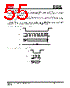
55 / 118 page  IS25LP032D IS25WP032D Integrated Silicon Solution, Inc.- www.issi.com 55 Rev. A12 08/04/2020 8.13 CHIP ERASE OPERATION (CER, C7h/60h) A Chip Erase (CER) instruction erases the entire memory array. Before the execution of CER instruction, the Write Enable Latch (WEL) must be set via a Write Enable (WREN) instruction. The WEL is automatically reset after completion of a chip erase operation. The CER instruction code is input via the SI. Erase operation will start immediately after CE# is pulled high, otherwise the CER instruction will not be executed. The internal control logic automatically handles the erase voltage and timing. Chip Erase (CER) instruction can be executed only when Block Protection (BP3~BP0) bits are set to 0s. If the BP bits are not 0, the CER command is not executed and E_ERR and PROT_E are set. Figure 8.20 Chip Erase Sequence In SPI Mode Instruction = C7h/60h CE# SCK SI 0 1 2 3 4 5 6 7 Mode 3 Mode 0 SO High Impedance Figure 8.21 Chip Erase Sequence In QPI Mode C7h/60h CE# SCK IO[3:0] 0 1 Mode 3 Mode 0 |
|
链接网址 |
| ALLDATASHEET是否为您带来帮助? [ DONATE ] |
关于 Alldatasheet | 广告服务 | 联系我们 | 隐私政策 | 数据表链接 | 链接交换 | 制造商名单 All Rights Reserved©Alldatasheet.com |
| Russian : Alldatasheetru.com | Korean : Alldatasheet.co.kr | Spanish : Alldatasheet.es | French : Alldatasheet.fr | Italian : Alldatasheetit.com Portuguese : Alldatasheetpt.com | Polish : Alldatasheet.pl | Vietnamese : Alldatasheet.vn Indian : Alldatasheet.in | Mexican : Alldatasheet.com.mx | British : Alldatasheet.co.uk | New Zealand : Alldatasheet.co.nz |
|
Family Site : ic2ic.com |
icmetro.com |
 Chinese ▼
 English
 Chinese
 German
 Japanese
 Russian
 Korean
 Spanish
 French
 Italian
 Portuguese
 Polish
 Vietnamese
 Indian
 Mexican
 British
 New Zealand