|
数据搜索系统,热门电子元器件搜索 |
|
|
数据搜索系统,热门电子元器件搜索 |
|
KSZ9563RNXC 数据表(PDF) 117 Page - Microchip Technology |
|
|
|||||||||||||||||||||||||||||
KSZ9563RNXC 数据表(HTML) 117 Page - Microchip Technology |
|
|
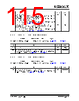
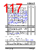
117 / 226 page  2017-2018 Microchip Technology Inc. DS00002419D-page 117 KSZ9563R 5.1.6.21 Trigger Output Unit Control 2 Register This register is indexed by the Trigger Unit Index Pointer value in bits [1:0] of the Global PTP Unit Index Register. 22:20 Trigger Event Output Signal Pattern (TRIGGER_PATTERN) To select a trigger event output when TRIG_EN=1 and the trigger target time has reached the system time: 000 = Generates negative edge (from default “H” -> “L” and stays “L”) 001 = Generates positive edge (from default “L” -> “H” and stays “H”) 010 = Generates negative pulse (from default “H” -> “L” pulse -> “H” and stays “H”). The pulse width is defined in the Trigger Output Unit Control 2 Register. 011 = Generates positive pulse (from default “L” -> “H” pulse -> “L” and stays “L”). The pulse width is defined in the Trigger Output Unit Control 2 Register. 100 = Generates negative periodic signal. The “L” pulse width is defined in the Trigger Output Unit Control 2 Register, the cycle width is defined in the Trigger Output Unit Control 3 Register and Trigger Output Unit Control 4 Register, and the number of cycles is defined in the Trigger Output Unit Control 5 Reg- ister (it is an infinite number if the number of cycles is zero). 101 = Generates positive periodic signal. The “H” pulse width is defined in the Trigger Output Unit Control 2 Register, the cycle width is defined in the Trigger Output Unit Control 3 Register and Trigger Output Unit Control 4 Register, and the number of cycles is defined in the Trigger Output Unit Control 5 Reg- ister (it is an infinite number if the number of cycles is zero). 110 = Generates output signal from the 16-bit pattern in the Trigger Output Unit Control 3 Register, which is shifted MSB fist and looped. Each bit width is defined in the Trigger Output Unit Control 3 Register and Trigger Output Unit Control 4 Register and the total number of bits to shift out is defined in the Trigger Output Unit Control 5 Register (it is infinite if this register value is zero). 111 = RESERVED. Note: The maximum output clock frequency is up to 12.5MHz. R/W 000b 19:17 RESERVED RO 000b 16 Trigger GPIO Selects one of the GPIO pins to serve this trigger output unit. The trigger out- put signals are OR’ed together to form a combined signal if multiple trigger output units are set to the same GPIO output pin. 1 = GPIO_2 0 = GPIO_1 R/W 0b 15:0 Trigger Output Iteration Count (TRIGGER_PATTERN_ITERATION) Defines the iteration count number to output the 16-bit trigger pattern defined in the Trigger Output Unit Control 3 Register in cascade mode at tail unit. For example, 0x0000 is 1 count and 0x000F is 16 counts. It is infinite if there is no tail unit in cascade mode. R/W 0x0000 Address: 0x053C - 0x053F Size: 32 bits Bits Description Type Default 31:0 Trigger Output Cycle Width or Bit Width (TRIGGER_CYCLE_WIDTH) Defines the cycle width for generating periodic signals. Each unit value equals 1ns. For example, the cycle width is 80ns if this register value is 80 (0x50). R/W 0x00000000 Bits Description Type Default |
|
链接网址 |
| ALLDATASHEET是否为您带来帮助? [ DONATE ] |
关于 Alldatasheet | 广告服务 | 联系我们 | 隐私政策 | 数据表链接 | 链接交换 | 制造商名单 All Rights Reserved©Alldatasheet.com |
| Russian : Alldatasheetru.com | Korean : Alldatasheet.co.kr | Spanish : Alldatasheet.es | French : Alldatasheet.fr | Italian : Alldatasheetit.com Portuguese : Alldatasheetpt.com | Polish : Alldatasheet.pl | Vietnamese : Alldatasheet.vn Indian : Alldatasheet.in | Mexican : Alldatasheet.com.mx | British : Alldatasheet.co.uk | New Zealand : Alldatasheet.co.nz |
|
Family Site : ic2ic.com |
icmetro.com |
 Chinese ▼
 English
 Chinese
 German
 Japanese
 Russian
 Korean
 Spanish
 French
 Italian
 Portuguese
 Polish
 Vietnamese
 Indian
 Mexican
 British
 New Zealand