|
数据搜索系统,热门电子元器件搜索 |
|
|
数据搜索系统,热门电子元器件搜索 |
|
M24M02-R 数据表(PDF) 23 Page - STMicroelectronics |
|
|
|||||||||||||||||||||||||||||
M24M02-R 数据表(HTML) 23 Page - STMicroelectronics |
|
|
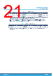
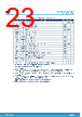
23 / 40 page  Table 13. 400 kHz AC characteristics Symbol Alt. Parameter(1) Min. Max. Unit fC fSCL Clock frequency - 400 kHz tCHCL tHIGH Clock pulse width high 600 - ns tCLCH tLOW Clock pulse width low 1300 - ns tQL1QL2(2) tF SDA (out) fall time 20(3) 120 ns tXH1XH2 tR Input signal rise time (4) (4) ns tXL1XL2 tF Input signal fall time (4) (4) ns tDXCH tSU:DAT Data in set up time 100 - ns tCLDX tHD:DAT Data in hold time 0 - ns tCLQX(5) tDH Data out hold time 100 - ns tCLQV(6) tAA Clock low to next data valid (access time) 100 900 ns tCHDL tSU:STA Start condition setup time 600 - ns tDLCL tHD:STA Start condition hold time 600 - ns tCHDH tSU:STO Stop condition set up time 600 - ns tDHDL tBUF Time between Stop condition and next Start condition 1300 - ns tWLDL(2)(7) tSU:WC WC set up time (before the Start condition) 0 - µs tDHWH(2)(8) tHD:WC WC hold time (after the Stop condition) 1 - µs tW tWR Write time - 10 ms tNS(2) - Pulse width ignored (input filter on SCL and SDA) - single glitch - 80 ns 1. Test conditions (in addition to those specified under Table 7 and Table 8). 2. Evaluated by characterization - Not tested in production. 3. With CL = 10 pF. 4. There is no min. or max. values for the input signal rise and fall times. It is however recommended by the I²C specification that the input signal rise and fall times be more than 20 ns and less than 300 ns when fC < 400 kHz. 5. The min value for tCLQX (Data out hold time) of the M24xxx devices offers a safe timing to bridge the undefined region of the falling edge SCL. 6. tCLQV is the time (from the falling edge of SCL) required by the SDA bus line to reach either 0.3 VCC or 0.7 VCC, assuming that Rbus × Cbus time constant is within the values specified in Figure 12. 7. WC=0 set up time condition to enable the execution of a WRITE command. 8. WC=0 hold time condition to enable the execution of a WRITE command. M24M02-DR M24M02-R DC and AC parameters DS7025 - Rev 11 page 23/40 |
|
链接网址 |
| ALLDATASHEET是否为您带来帮助? [ DONATE ] |
关于 Alldatasheet | 广告服务 | 联系我们 | 隐私政策 | 数据表链接 | 链接交换 | 制造商名单 All Rights Reserved©Alldatasheet.com |
| Russian : Alldatasheetru.com | Korean : Alldatasheet.co.kr | Spanish : Alldatasheet.es | French : Alldatasheet.fr | Italian : Alldatasheetit.com Portuguese : Alldatasheetpt.com | Polish : Alldatasheet.pl | Vietnamese : Alldatasheet.vn Indian : Alldatasheet.in | Mexican : Alldatasheet.com.mx | British : Alldatasheet.co.uk | New Zealand : Alldatasheet.co.nz |
|
Family Site : ic2ic.com |
icmetro.com |
 Chinese ▼
 English
 Chinese
 German
 Japanese
 Russian
 Korean
 Spanish
 French
 Italian
 Portuguese
 Polish
 Vietnamese
 Indian
 Mexican
 British
 New Zealand