|
数据搜索系统,热门电子元器件搜索 |
|
|
数据搜索系统,热门电子元器件搜索 |
|
P9242-R 数据表(PDF) 25 Page - Renesas Technology Corp |
|
|
|||||||||||||||||||||||||||||
P9242-R 数据表(HTML) 25 Page - Renesas Technology Corp |
|
|
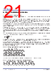
25 / 38 page  P9242-R Datasheet © 2018 Integrated Device Technology, Inc 25 January 16, 2018 10. Functional Registers The P9242-R registers can be read and written to via the P9242-R’s I2C interface on the SCL and SDA pins. Section 10.1 defines the protocol for reading and writing via this interface. Section 10.2 gives the details for the register definitions. 10.1 I2C Interface Figure 24. I2C Access Read Protocol and Write Protocol From Master From Slave ACK ACK ACK DataByte_1 A A DataByte_3 A 818181 ACK DataByte_0 A 81 Clocks . . . . DataByte_2 Start 61HEX 61HEX ACK 06HEX ACK 80HEX ACK ACK R/W R/W S Slave Address Sr Slave Address A Memory Address MSB 0 A Memory Address LSB A 1 A . . . . 17 7 18181 1 1 1 Clocks Read Protocol P ACK ACK CmdByte_1 A A CmdFlag_1 818181 ACK CmdByte_0 A 81 Clocks CmdFlag_0 A/A 1 NAK LSB = Least Significant Byte MSB = Most Significant Byte A = Acknowledge (SDA LOW) A = Not Acknowledge (SDA HIGH) S = Start Condition Sr = Restart Condition P = Stop Condition |
|
链接网址 |
| ALLDATASHEET是否为您带来帮助? [ DONATE ] |
关于 Alldatasheet | 广告服务 | 联系我们 | 隐私政策 | 数据表链接 | 链接交换 | 制造商名单 All Rights Reserved©Alldatasheet.com |
| Russian : Alldatasheetru.com | Korean : Alldatasheet.co.kr | Spanish : Alldatasheet.es | French : Alldatasheet.fr | Italian : Alldatasheetit.com Portuguese : Alldatasheetpt.com | Polish : Alldatasheet.pl | Vietnamese : Alldatasheet.vn Indian : Alldatasheet.in | Mexican : Alldatasheet.com.mx | British : Alldatasheet.co.uk | New Zealand : Alldatasheet.co.nz |
|
Family Site : ic2ic.com |
icmetro.com |
 Chinese ▼
 English
 Chinese
 German
 Japanese
 Russian
 Korean
 Spanish
 French
 Italian
 Portuguese
 Polish
 Vietnamese
 Indian
 Mexican
 British
 New Zealand