|
数据搜索系统,热门电子元器件搜索 |
|
|
数据搜索系统,热门电子元器件搜索 |
|
ADL5519ACPZ-R2 数据表(PDF) 27 Page - Analog Devices |
|
|
|||||||||||||||||||||||||||||
ADL5519ACPZ-R2 数据表(HTML) 27 Page - Analog Devices |
|
|
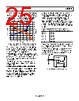
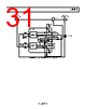
27 / 39 page  Data Sheet ADL5519 Rev. C | Page 27 of 39 OUTPUT FILTERING Accurate power detection for signals with RF bursts is achieved when the ADL5519 is able to respond quickly to the change in RF power. For applications in which maximum video bandwidth and, consequently, fast rise time are desired, it is essential that the CLPA, CLPB pins have very little capacitance on them (some capacitance reduces the ringing). The nominal output video bandwidth of 10 MHz can be reduced by connecting a ground-referenced capacitor (CFLT) to the CLPA, CLPB pins, as shown in Figure 65. This is generally done to reduce output ripple (at twice the input frequency for a symmetric input waveform, such as a sinusoidal signal). ILOGA, ILOGB CFLT 1.5kΩ OUTA, OUTB CLPA, CLPB 3.5pF ADL5519 +4 Figure 65. Lowering the Post Demodulation Bandwidth CFLT is selected using the following equation: pF 5 . 3 k 5 . 1 1 Bandwidth Video C FLT (12) The video bandwidth should typically be set to a frequency less than or equal to approximately 1/10 the minimum input frequency. There are no problems with putting large capacitor values on the CLPA, CLPB pins. These large capacitor values ensure that the output ripple of the demodulated log output, which is at twice the input frequency, is well filtered. Signals with modulation may need additional filtering (a larger CFLT capacitance) to remove modulation bleedthrough. PACKAGE CONSIDERATIONS The ADL5519 uses a compact, 32-lead LFCSP. A large exposed paddle on the bottom of the device provides both a thermal benefit and a low inductance path to ground for the circuit. To make proper use of this packaging feature, the PCB RF/dc common-ground reference needs to make contact with the paddle with as many vias as possible to lower inductance and thermal impedance. OPERATION ABOVE 8 GHz The ADL5519 is specified for operation up to 8 GHz, but it provides useful measurement accuracy over a reduced dynamic range of up to 10 GHz. Figure 66 shows the performance of the ADL5519 over temperature for a input frequency of 10 GHz. This high frequency performance is achieved using the configu- ration shown in Figure 53. The dynamic range shown is reduced from the typical device performance, but the ADL5519 can provide 30 dB of measurement range with less than 3 dB of linearity error. Implementing an impedance match for frequencies greater than 8 GHz can improve the sensitivity of the ADL5519 and its measurement range. 2.00 1.75 1.50 1.25 1.00 0.75 0.50 0.25 0 4.0 3.0 2.0 1.0 0 –1.0 –2.0 –3.0 –4.0 –40 –35 –30 –25 –20 –15 –10 –5 0 PIN (dBm) Figure 66. VOUT and Log Conformance vs. Input Amplitude at 10 GHz, Over Temperature, ADJA, ADJB = 1.8 V, 1.8 V |
|
链接网址 |
| ALLDATASHEET是否为您带来帮助? [ DONATE ] |
关于 Alldatasheet | 广告服务 | 联系我们 | 隐私政策 | 数据表链接 | 链接交换 | 制造商名单 All Rights Reserved©Alldatasheet.com |
| Russian : Alldatasheetru.com | Korean : Alldatasheet.co.kr | Spanish : Alldatasheet.es | French : Alldatasheet.fr | Italian : Alldatasheetit.com Portuguese : Alldatasheetpt.com | Polish : Alldatasheet.pl | Vietnamese : Alldatasheet.vn Indian : Alldatasheet.in | Mexican : Alldatasheet.com.mx | British : Alldatasheet.co.uk | New Zealand : Alldatasheet.co.nz |
|
Family Site : ic2ic.com |
icmetro.com |
 Chinese ▼
 English
 Chinese
 German
 Japanese
 Russian
 Korean
 Spanish
 French
 Italian
 Portuguese
 Polish
 Vietnamese
 Indian
 Mexican
 British
 New Zealand