|
数据搜索系统,热门电子元器件搜索 |
|
|
数据搜索系统,热门电子元器件搜索 |
|
ADL5519ACPZ-R2 数据表(PDF) 10 Page - Analog Devices |
|
|
|||||||||||||||||||||||||||||
ADL5519ACPZ-R2 数据表(HTML) 10 Page - Analog Devices |
|
|
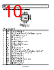
10 / 39 page  ADL5519 Data Sheet Rev. C | Page 10 of 39 PIN CONFIGURATION AND FUNCTION DESCRIPTIONS COMR COMR VPSB ADJB VREF VLVL CLPB VSTB COMR COMR VPSA ADJA VPSR TEMP CLPA VSTA NOTES 1. NC = NO CONNECT. 2. EXPOSED PAD MUST BE INTERNALLY CONNECTED TO COMR. 24 23 22 21 20 19 18 17 1 2 3 4 5 6 7 8 ADL5519 TOP VIEW (Not to Scale) Figure 2. Pin Configuration Table 3. Pin Function Descriptions Pin No. Mnemonic Description 1 COMR Connect via low impedance to common. 2 COMR Connect via low impedance to common. 3 VPSB Positive Supply for Channel B. Apply 3.3 V to 5.5 V supply voltage. 4 ADJB Dual-Function Pin: Temperature Adjust Pin for Channel B and Power-Down Interface for OUTB. 5 VREF Voltage Reference (1.15 V). 6 VLVL DC Common-Mode Adjust for Difference Output. 7 CLPB Loop Filter Pin for Channel B. 8 VSTB Setpoint Control Input for Channel B. 9 NC No Connect. 10 OUTB Output Voltage for Channel B. 11 FBKB Difference Op Amp Feedback Pin for OUTN Op Amp. 12 OUTN Difference Output (OUTB − OUTA + VLVL). 13 OUTP Difference Output (OUTA − OUTB + VLVL). 14 FBKA Difference Op Amp Feedback Pin for OUTP Op Amp. 15 OUTA Output Voltage for Channel A. 16 NC No Connect. 17 VSTA Setpoint Control Input for Channel A. 18 CLPA Loop Filter Pin for Channel A. 19 TEMP Temperature Sensor Output (1.3 V with 4.5 mV/°C Slope). 20 VPSR Positive Supply for Difference Outputs and Temperature Sensor. Apply 3.3 V to 5.5 V supply voltage. 21 ADJA Dual-Function Pin: Temperature Adjust Pin for Channel A and Power-Down Interface for OUTA. 22 VPSA Positive Supply for Channel A. Apply 3.3 V to 5.5 V supply voltage. 23 COMR Connect via low impedance to common. 24 COMR Connect via low impedance to common. 25 INHA AC-Coupled RF Input for Channel A. 26 INLA AC-Coupled RF Common for Channel A. 27 COMR Connect via low impedance to common. 28 PWDN Power-Down for Difference Output and Temperature Sensor. 29 COMR Connect via low impedance to common. 30 COMR Connect via low impedance to common. 31 INLB AC-Coupled RF Common for Channel B. 32 INHB AC-Coupled RF Input for Channel B. Paddle Internally connected to COMR. |
|
链接网址 |
| ALLDATASHEET是否为您带来帮助? [ DONATE ] |
关于 Alldatasheet | 广告服务 | 联系我们 | 隐私政策 | 数据表链接 | 链接交换 | 制造商名单 All Rights Reserved©Alldatasheet.com |
| Russian : Alldatasheetru.com | Korean : Alldatasheet.co.kr | Spanish : Alldatasheet.es | French : Alldatasheet.fr | Italian : Alldatasheetit.com Portuguese : Alldatasheetpt.com | Polish : Alldatasheet.pl | Vietnamese : Alldatasheet.vn Indian : Alldatasheet.in | Mexican : Alldatasheet.com.mx | British : Alldatasheet.co.uk | New Zealand : Alldatasheet.co.nz |
|
Family Site : ic2ic.com |
icmetro.com |
 Chinese ▼
 English
 Chinese
 German
 Japanese
 Russian
 Korean
 Spanish
 French
 Italian
 Portuguese
 Polish
 Vietnamese
 Indian
 Mexican
 British
 New Zealand