|
数据搜索系统,热门电子元器件搜索 |
|
|
数据搜索系统,热门电子元器件搜索 |
|
ADL5902ACPZ-R2 数据表(PDF) 17 Page - Analog Devices |
|
|
|||||||||||||||||||||||||||||
ADL5902ACPZ-R2 数据表(HTML) 17 Page - Analog Devices |
|
|
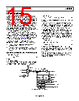
17 / 28 page  Data Sheet ADL5902 Rev. B | Page 17 of 28 SMALL SIGNAL LOOP RESPONSE The ADL5902 uses a VGA in a loop to force a squared RF signal to be equal to a squared dc voltage. This nonlinear loop can be simplified and solved for a small signal loop response. The low- pass corner pole is given by FreqLP ≈ 1.83 × ITGT/(CLPF) (12) where: ITGT is in amperes. CLPF is in farads. FreqLP is in hertz. ITGT is derived from VTGT; however, ITGT is a squared value of VTGT multiplied by a transresistance, namely ITGT = gm × VTGT2 (13) gm is approximately 18.9 μs; therefore, with VTGT equal to the typically recommended 0.8 V, ITGT is approximately 12 μA. The value of this current varies with temperature; therefore, the small signal pole varies with temperature. However, because the RF squaring circuit and dc squaring circuit track with temperature, there is no temperature variation contribution to the absolute value of VOUT. For CW signals, FreqLP ≈ 67.7 × 10⁻⁶/(CLPF) (14) However, signals with large crest factors include low pseudo- random frequency content that must be either filtered out or sampled and averaged out (see the Choosing a Value for CLPF section for more information). TEMPERATURE SENSOR INTERFACE The ADL5902 provides a temperature sensor output with a scaling factor of the output voltage of approximately 4.9 mV/°C. The output is capable of sourcing 4 mA and sinking 50 μA maximum at 25°C. An external resistor can be connected from TEMP to COMM to provide additional current sink capability. The typical output voltage at 25°C is approximately 1.4 V. TEMP VPOS COMM INTERNAL VPAT 12kΩ 4kΩ Figure 38. TEMP Interface Simplified Schematic VREF INTERFACE The VREF pin provides an internally generated voltage reference for the user. The VREF voltage is a temperature stable 2.3 V reference that is capable of sourcing 4 mA and sinking 50 μA maximum. An external resistor can be connected from VREF to COMM to provide additional current sink capability. The voltage on this pin can drive the TADJ/PWDN and VTGT pins. INTERNAL VOLTAGE 16kΩ VREF VPOS COMM Figure 39. VREF Interface Simplified Schematic TEMPERATURE COMPENSATION INTERFACE While the ADL5902 has a highly stable measurement output with respect to temperature using proprietary techniques, for optimal performance, the output temperature drift must be compensated for using the TADJ pin. The absolute value of compensation varies with frequency and VTGT. Table 4 shows the recommended voltages for VTADJ to maintain a temperature drift error of typically ±0.5 dB or better over the intended temperature range (−40°C < TA < +85°C) when driven single-ended and VTGT = 0.8 V. Table 4. Recommended VTADJ for Selected Frequencies Frequency VTADJ (V) R9 in Figure 54 (Ω) R12 in Figure 54 (Ω) 100 MHz 0.5 1430 402 700 MHz 0.4 1430 301 900 MHz 0.4 1430 301 1.9 GHz 0.4 1430 301 2.14 GHz 0.4 1430 301 2.6 GHz 0.45 1430 348 3.5 GHz 0.5 1430 402 5.8 GHz 0.95 1430 1007 The values in Table 4 are chosen to give the best drift performance at the high end of the usable dynamic range over the −40°C to +85°C temperature range. There is often a trade off in setting values, and optimizing for one area of the dynamic range can mean less than optimal drift performance at other input amplitudes. |
|
|
链接网址 |
| ALLDATASHEET是否为您带来帮助? [ DONATE ] |
关于 Alldatasheet | 广告服务 | 联系我们 | 隐私政策 | 数据表链接 | 链接交换 | 制造商名单 All Rights Reserved©Alldatasheet.com |
| Russian : Alldatasheetru.com | Korean : Alldatasheet.co.kr | Spanish : Alldatasheet.es | French : Alldatasheet.fr | Italian : Alldatasheetit.com Portuguese : Alldatasheetpt.com | Polish : Alldatasheet.pl | Vietnamese : Alldatasheet.vn Indian : Alldatasheet.in | Mexican : Alldatasheet.com.mx | British : Alldatasheet.co.uk | New Zealand : Alldatasheet.co.nz |
|
Family Site : ic2ic.com |
icmetro.com |
 Chinese ▼
 English
 Chinese
 German
 Japanese
 Russian
 Korean
 Spanish
 French
 Italian
 Portuguese
 Polish
 Vietnamese
 Indian
 Mexican
 British
 New Zealand