|
数据搜索系统,热门电子元器件搜索 |
|
|
数据搜索系统,热门电子元器件搜索 |
|
ADL5906SCPZN-R7 数据表(PDF) 28 Page - Analog Devices |
|
|
|||||||||||||||||||||||||||||
ADL5906SCPZN-R7 数据表(HTML) 28 Page - Analog Devices |
|
|
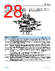
28 / 30 page  Data Sheet ADL5906 EVALUATION BOARD analog.com Rev. B | 28 of 30 The ADL5906-EVALZ is a fully populated, 4-layer, FR4-based eval- uation board. For normal operation, it requires a 5 V/100 mA power supply. The 5 V power supply must be connected to the VPOS and GND test loops. The RF input signal is applied to the SMA connec- tor (RFIN). The output voltage is available on the SMA connector (VOUT1) or on the test loop (VOUT). Configuration options for the evaluation board are listed in Table 8. Figure 63. Evaluation Board Schematic Table 8. Evaluation Board Configuration Options Component Function/Notes Default Value RFIN, R3, C10, C12 RF input. The evaluation board is configured for single-ended drive on the RFIN+ pin (Pin 14). Capacitors C10 and C12 have been set large enough so that the full frequency range of the device is covered. If operation down to 10 MHz is not required, the value of these capacitors can be reduced. RFIN = SMA connector, C10 = C12 = 10 nF, R3 = 60.4 Ω VTGT, R10, R11 VTGT interface. R10 and R11 are set up to provide 0.8 V to VTGT derived from VREF. If R10 and R11 are removed, an external voltage can be applied on the VTGT test point. VTGT = black test loop, R10 = 3.74 kΩ, R11 = 2 kΩ, VTGT = 0.8 V VPOS, GND, C3, C4, C5,C7 Power supply interface and decoupling. Apply the power supply for the evaluation board to the VPOS and GND test loops. The nominal supply decoupling consists of a 100 pF capacitor and a 0.1 µF capacitor on each power supply pin, with the 100 pF capacitor placed closer to the pin. VPOS = red test loop, GND = black test loop, C3 = C7 = 0.1 µF, C4 = C5 = 100 pF VOUT, VOUT1, VSET, R1, R2, R6, R15 Output interface. In measurement mode, a portion of the voltage at the VRMS pin is fed back to the VSET pin via R6 (R6 is normally set to 0 Ω). Using the voltage divider created by R2 and R6, the magnitude of the slope of VRMS is increased by reducing the portion of VRMS that is fed back to VSET. Resistors R1 and R15 can be used to reduce the output slope. VOUT = black test loop, VOUT1 = SMA connector, VSET = black test loop, R1 = R6 = 0 Ω, R15 = R2 = open In controller mode, R6 must be open. In this mode, the ADL5906 can control the gain of a variable gain amplifier (VGA) or voltage variable attenuator (VVA). A setpoint voltage is applied to the VSET test loop, and the VRMS test loop or SMA connector drives the gain control input of the VGA/VVA. C9 RMS averaging capacitor. The value of the rms averaging capacitor should be set based on the peak-to-average ratio of the input signal and based on the desired output response time and residual output noise. C9 = 0.1 µF TC2, R9, R12 TADJ/PWDN interface. The TADJ/PWDN pin controls the slope temperature compensation and/or shuts down the device. The evaluation board is configured with VTADJ connected to VREF through a resistor divider (R9, R12). This voltage divider can be removed (or simply overdriven) allowing for the external application of a voltage to the VTADJ pin by applying a voltage to the TC2 test point. TC2 = black test loop, R9 = 1.5 kΩ, R12 = 270 Ω, VTADJ = 0.35 V |
|
|
链接网址 |
| ALLDATASHEET是否为您带来帮助? [ DONATE ] |
关于 Alldatasheet | 广告服务 | 联系我们 | 隐私政策 | 数据表链接 | 链接交换 | 制造商名单 All Rights Reserved©Alldatasheet.com |
| Russian : Alldatasheetru.com | Korean : Alldatasheet.co.kr | Spanish : Alldatasheet.es | French : Alldatasheet.fr | Italian : Alldatasheetit.com Portuguese : Alldatasheetpt.com | Polish : Alldatasheet.pl | Vietnamese : Alldatasheet.vn Indian : Alldatasheet.in | Mexican : Alldatasheet.com.mx | British : Alldatasheet.co.uk | New Zealand : Alldatasheet.co.nz |
|
Family Site : ic2ic.com |
icmetro.com |
 Chinese ▼
 English
 Chinese
 German
 Japanese
 Russian
 Korean
 Spanish
 French
 Italian
 Portuguese
 Polish
 Vietnamese
 Indian
 Mexican
 British
 New Zealand