|
数据搜索系统,热门电子元器件搜索 |
|
|
数据搜索系统,热门电子元器件搜索 |
|
ADL5906SCPZN-R7 数据表(PDF) 20 Page - Analog Devices |
|
|
|||||||||||||||||||||||||||||
ADL5906SCPZN-R7 数据表(HTML) 20 Page - Analog Devices |
|
|
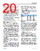
20 / 30 page  Data Sheet ADL5906 THEORY OF OPERATION analog.com Rev. B | 20 of 30 forms of modulation with respect to the ideal CW line. This method for calculating error is accurate, assuming that each device is calibrated at room temperature. In the second plot format, the VRMS voltage at a given input ampli- tude and temperature is subtracted from the corresponding VRMS at 25°C and then divided by the 25°C slope to obtain an error in decibels. This type of plot does not provide any information on the linear-in-dB performance of the device; it merely shows the decibel equivalent of the deviation of VRMS over temperature, given a calibration at 25°C. When calculating error from any one particular calibration point, this error format is accurate. It is accurate over the full range shown on the plot assuming that enough calibration points are used. Figure 12 shows this plot type. The error calculations for Figure 34 are similar to those for the VRMS plots. The slope and intercept of the VTEMP function vs. temperature are determined and applied as follows: Error (°C) = (VTEMP − Slope × (Temp − TZ))/Slope (10) where: VTEMP is the voltage at the TEMP pin at that temperature. Slope is, typically, 4.8 mV/°C. Temp is the ambient temperature of the ADL5906 in degrees Celsius. TZ is the x-axis intercept expressed in degrees Celsius (the temper- ature that would result in a VTEMP of 0 V if this were possible). MEASUREMENT MODE BASIC CONNECTIONS The basic connections circuit for ADL5906 is shown in Figure 51. The ADL5906 requires a single supply of nominally 5 V. The supply is connected to the VPOS1 and VPOS2 supply pins. Decouple each of these pins using two capacitors with values equal or similar to those shown in Figure 51. Place these capacitors as close as possible to the VPOS pins. The three no connect pins (NIC) are not internally connected. Leave these pins unconnected. An external 60.4 Ω resistor combines with the relatively high RF input impedance of the ADL5906 to provide a broadband 50 Ω match. Place an ac coupling capacitor between this resistor and RFIN+. AC-couple the RFIN− input to ground using the same value capacitor. To operate down to 10 MHz, the coupling capacitors must be at least 100 pF. The ADL5906 is placed in measurement mode by connecting the VRMS pin to the VSET pin. In measurement mode, the output voltage is proportional to the log of the rms input signal level. SETTING VTADJ As described in the Theory of Operation section, the output temper- ature drift can be compensated by applying a voltage to the TADJ pin. The compensating voltage varies with frequency. The voltage for the TADJ pin can be easily derived from a resistor divider connected to the VREF pin. Table 4 shows the recommended VTADJ voltages for operation from −55°C to +125°C, along with resistor divider values. Resistor values are chosen so that they neither pull too much current from the VREF pin (IOUTMAX = 4 mA) nor are so large that the maximum bias current at a VTADJ = 1 V (14 µA) affects the resulting voltage. The VTADJ function provides temperature compensation of the out- put slope of the ADL5906. The Using VTEMP to Improve Intercept Temperature Drift section describes how the temperature stability of the ADL5906 can be further improved. Recommended VTADJ Voltages Table 4. Frequency VTADJ (V) R9 (Ω) R12 (Ω) 10 MHz to 2.14 GHz 0.35 1500 270 2.6 GHz 0.4 1500 316 3.5 GHz 0.45 1500 365 5.8 GHz 1.0 1540 1200 8 GHz 1.0 1540 1200 10 GHz 1.0 1540 1200 SETTING VTGT As described in the Theory of Operation section, setting the voltage on VTGT to 0.8 V represents a compromise between achieving excellent rms accuracy and maximizing dynamic range. The voltage on VTGT can be derived from the VREF pin using a resistor divider, as shown Figure 51. Like the resistors chosen to set the VTADJ voltage, the resistors setting VTGT must have reasonable values that do not pull too much current from VREF or cause bias current errors. In addition, note the combined current that VREF must deliver to generate the VTADJ and VTGT voltages. The values shown in Figure 51 and Table 4 result in a maximum VREF current of 1.7 mA. This current is well below the maximum specified VREF current of 4 mA. CHOOSING A VALUE FOR CRMS CRMS provides the averaging function for the internal rms compu- tation. Using the minimum value for CRMS allows the quickest response time to a pulsed waveform but leaves significant output noise on the output voltage signal. By the same token, a large filter capacitor reduces output noise but at the expense of response time. In applications where response time is not critical, a relatively large capacitor can be placed on the CRMS pin. In Figure 51, a value of 0.1 µF is used. For most signal modulation schemes, this value ensures excellent rms measurement compliance and low residual output noise. There is no maximum capacitance limit for CRMS. Figure 50 shows how output noise varies with CRMS when the ADL5906 is driven by a single-carrier W-CDMA signal (Test Model TM1-64, peak envelope power = 10.56 dB, bandwidth = 3.84 MHz). |
|
|
链接网址 |
| ALLDATASHEET是否为您带来帮助? [ DONATE ] |
关于 Alldatasheet | 广告服务 | 联系我们 | 隐私政策 | 数据表链接 | 链接交换 | 制造商名单 All Rights Reserved©Alldatasheet.com |
| Russian : Alldatasheetru.com | Korean : Alldatasheet.co.kr | Spanish : Alldatasheet.es | French : Alldatasheet.fr | Italian : Alldatasheetit.com Portuguese : Alldatasheetpt.com | Polish : Alldatasheet.pl | Vietnamese : Alldatasheet.vn Indian : Alldatasheet.in | Mexican : Alldatasheet.com.mx | British : Alldatasheet.co.uk | New Zealand : Alldatasheet.co.nz |
|
Family Site : ic2ic.com |
icmetro.com |
 Chinese ▼
 English
 Chinese
 German
 Japanese
 Russian
 Korean
 Spanish
 French
 Italian
 Portuguese
 Polish
 Vietnamese
 Indian
 Mexican
 British
 New Zealand