|
数据搜索系统,热门电子元器件搜索 |
|
|
数据搜索系统,热门电子元器件搜索 |
|
ADL5906SCPZN-R7 数据表(PDF) 19 Page - Analog Devices |
|
|
|||||||||||||||||||||||||||||
ADL5906SCPZN-R7 数据表(HTML) 19 Page - Analog Devices |
|
|
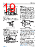
19 / 30 page  Data Sheet ADL5906 THEORY OF OPERATION analog.com Rev. B | 19 of 30 wake-up response varies depending on the input coupling and the value of CRMS. Figure 46. TADJ/PWDN Interface Simplified Schematic VSET INTERFACE The VSET interface has a high input impedance of 72 kΩ. The voltage at VSET is converted to an internal current used to set the internal VGA gain. The VGA attenuation control is approximately 18 dB/V. Figure 47. VSET Interface Simplified Schematic OUTPUT INTERFACE The ADL5906 incorporates rail-to-rail output drivers with pull-up and pull-down capabilities. The level shift circuitry and the output ampli- fier are very fast compared to the typical rms response required by a complex waveform. In essence, the output stage from the CRMS pin to the VRMS output is only a dc signal because by definition VRMS is supposed to be a single rms value. The VRMS pin can source and sink up to 10 mA. Figure 48. VRMS Interface Simplified Schematic VTGT INTERFACE The target voltage can be set with an external source or by con- necting the VREF pin (nominally 2.3 V) to the VTGT pin through a resistive voltage divider. With 0.8 V on the VTGT pin, the rms voltage that must be provided by the VGA to balance the AGC feedback loop is 0.8 V × 0.05 = 40 mV rms. Most of the characteri- zation information in this data sheet was collected at VTGT = 0.8 V. Voltages higher and lower than this can be used; however, doing so increases or decreases the gain at the internal squaring cell, which results in a corresponding increase or decrease in intercept. This, in turn, affects the sensitivity and the usable measurement range, in addition to the sensitivity to different carrier modulation schemes. As VTGT decreases, the squaring circuits produce more noise; this becomes noticeable in the output response at low input signal amplitudes. As VTGT increases, measurement error due to modulation increases, and temperature drift tends to decrease. The chosen VTGT value of 0.8 V represents a compromise between these characteristics. Figure 49. VTGT Interface BASIS FOR ERROR CALCULATIONS The slope and intercept used in the error plots are calculated using the coefficients of a linear regression performed on data collected in its central operating range. The error plots in the Typical Perform- ance Characteristics section are shown in two formats: error from the ideal line and error with respect to the 25°C output voltage. The error from the ideal line is the decibel difference in VRMS from the ideal straight-line fit of VRMS calculated by the linear regression fit over the linear range of the detector, typically at 25°C. The error in decibels is calculated by Error (dB) = (VRMS − Slope × (PIN − PZ))/Slope (9) where PZ is the x-axis intercept expressed in decibels relative to 1 mW (the input amplitude that produces a 0 V output if such an output were possible). The error from the ideal line is not a measure of absolute accuracy because it is calculated using the slope and intercept of each device. However, it verifies the linearity and the effect of tempera- ture and modulation on the response of the device. An example of this type of plot is Figure 9. The slope and intercept that form the ideal line are those at 25°C with CW modulation. Figure 4, Figure 5, Figure 7, and Figure 8 show the error with various popular |
|
|
链接网址 |
| ALLDATASHEET是否为您带来帮助? [ DONATE ] |
关于 Alldatasheet | 广告服务 | 联系我们 | 隐私政策 | 数据表链接 | 链接交换 | 制造商名单 All Rights Reserved©Alldatasheet.com |
| Russian : Alldatasheetru.com | Korean : Alldatasheet.co.kr | Spanish : Alldatasheet.es | French : Alldatasheet.fr | Italian : Alldatasheetit.com Portuguese : Alldatasheetpt.com | Polish : Alldatasheet.pl | Vietnamese : Alldatasheet.vn Indian : Alldatasheet.in | Mexican : Alldatasheet.com.mx | British : Alldatasheet.co.uk | New Zealand : Alldatasheet.co.nz |
|
Family Site : ic2ic.com |
icmetro.com |
 Chinese ▼
 English
 Chinese
 German
 Japanese
 Russian
 Korean
 Spanish
 French
 Italian
 Portuguese
 Polish
 Vietnamese
 Indian
 Mexican
 British
 New Zealand