|
数据搜索系统,热门电子元器件搜索 |
|
|
数据搜索系统,热门电子元器件搜索 |
|
ADL5906SCPZN-R7 数据表(PDF) 8 Page - Analog Devices |
|
|
|||||||||||||||||||||||||||||
ADL5906SCPZN-R7 数据表(HTML) 8 Page - Analog Devices |
|
|
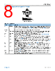
8 / 30 page  Data Sheet ADL5906 PIN CONFIGURATION AND FUNCTION DESCRIPTIONS analog.com Rev. B | 8 of 30 Figure 2. Pin Configuration Table 3. Pin Function Descriptions Pin No. Mnemonic Description 1 TADJ/PWDN Temperature Compensation/Shutdown. This is a dual function pin used for controlling temperature slope compensation at voltages <1.0 V and/or for shutting down the device at voltages >1.4 V. The temperature compensation voltage is generally set by connecting this pin to VREF through a resistive voltage divider (see the Setting VTADJ section for additional information). See Figure 46 for an equivalent circuit. 2, 13, 16 NIC No Internal Connection. Do not connect to these pins. These pins are not internally connected. 3, 10 VPOS1, VPOS2 Power Supply. Because these pins are internally shorted, they must be connected to the same 5 V power supply. The power supply to each pin must also be decoupled using 100 pF and 100 nF capacitors located as close as possible to the pins. 4, 9 GND1, GND2 Ground. Connect both GND1 and GND2 to system ground using a low impedance path. 5 CRMS RMS Averaging Capacitor. Connect an rms averaging capacitor between CRMS and ground. See the Choosing a Value for CRMS section for more information. See Figure 48 for an equivalent circuit. 6 VRMS RMS Output. In measurement mode, this pin is connected to VSET either directly or through a resistor divider (when the slope is being increased). In controller mode, this pin is used to drive the gain control input of a voltage variable attenuator (VVA) or variable gain amplifier (VGA). See Figure 48 for an equivalent circuit. 7 VSET Setpoint Input. In measurement mode, this pin is connected to VRMS either directly or through a resistor divider. In controller mode, the voltage applied to this pin sets the decibel value of the required RF input level to balance the automatic power control loop. See Figure 47 for an equivalent circuit. 8 VTEMP Temperature Sensor Output of 1.4 V at 25°C with a Coefficient of 4.8 mV/°C. See Figure 43 for an equivalent circuit. 11 VREF Reference Voltage Output. This voltage reference has a nominal value of 2.3 V. This reference output voltage can be used to set the voltage to the TADJ/PWDN and VTGT pins. See Figure 44 for an equivalent circuit. For optimal performance, bypass the VREF pin with a minimum capacitance of 1 nF to ground. 12 VTGT RMS Target Voltage. The voltage applied to this pin sets the target RF input at the output of the VGA that is also the rms squaring circuit. The recommended voltage for VTGT is 0.8 V. Increasing VTGT above 0.8 V degrades the rms accuracy of the ADL5906. Reducing VTGT below 0.8 V can improve the rms accuracy for signals with very high crest factors; however, it reduces the detection range of the ADL5906. See Figure 49 for an equivalent circuit. 14, 15 RFIN+, RFIN− RF Inputs. The RF inputs are normally applied single-ended with the RF input signal ac-coupled to RFIN+ and RFIN− ac-coupled to ground. See Figure 42 for an equivalent circuit. EPAD The exposed pad on the underside of the device (EPAD) is also internally connected to ground and requires a good thermal and electrical connection to the ground of the printed circuit board (PCB). |
|
|
链接网址 |
| ALLDATASHEET是否为您带来帮助? [ DONATE ] |
关于 Alldatasheet | 广告服务 | 联系我们 | 隐私政策 | 数据表链接 | 链接交换 | 制造商名单 All Rights Reserved©Alldatasheet.com |
| Russian : Alldatasheetru.com | Korean : Alldatasheet.co.kr | Spanish : Alldatasheet.es | French : Alldatasheet.fr | Italian : Alldatasheetit.com Portuguese : Alldatasheetpt.com | Polish : Alldatasheet.pl | Vietnamese : Alldatasheet.vn Indian : Alldatasheet.in | Mexican : Alldatasheet.com.mx | British : Alldatasheet.co.uk | New Zealand : Alldatasheet.co.nz |
|
Family Site : ic2ic.com |
icmetro.com |
 Chinese ▼
 English
 Chinese
 German
 Japanese
 Russian
 Korean
 Spanish
 French
 Italian
 Portuguese
 Polish
 Vietnamese
 Indian
 Mexican
 British
 New Zealand