|
数据搜索系统,热门电子元器件搜索 |
|
|
数据搜索系统,热门电子元器件搜索 |
|
PPC440SPE-RNB667C 数据表(PDF) 12 Page - Applied Micro Circuits Corporation |
|
|
|||||||||||||||||||||||||||||
PPC440SPE-RNB667C 数据表(HTML) 12 Page - Applied Micro Circuits Corporation |
|
|
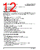
12 / 80 page  PowerPC 440SPe Embedded Processor 12 AMCC Proprietary Revision 1.23 - Sept 21, 2006 Preliminary Data Sheet • PCI-X initialization sequence support (frequency & mode determination) • Support for unexpected split completions • Outbound transaction split discard timers • Vital Product Data (VPD) support • PCI-X to PCI-Express opaque bridge DDR1/DDR2 SDRAM Memory Controller The DDR2 SDRAM memory controller supports industry standard 184-pin DIMMs, SO-DIMMs, and other discrete devices. Global memory timings, address and bank sizes, and memory addressing modes are programmable. The DDR2 SDRAM controller interfaces to the PLB through a Memory Queue (MQ) function that includes six high- speed 1KB FIFO buffers. Features include: • Registered and non-registered industry standard DIMMs • DDR2 400/667 support • 64-and 32-bit memory interfaces with optional 8-bit ECC (SEC/DED) • 5.32GB/s peak bandwidth for the 64-bit interface • 2.66GB/s peak bandwidth for the 32-bit interface • Four chip (bank) select signals supporting 4 external banks • CAS latencies of 2, 3, 4, 5, 6, and 7 supported • Page mode accesses (up to 32 open pages) with configurable paging policy • Look-ahead request queue with programmable depth of four commands. • Optional optimized command scheduling (activate/precharge non-conflicting banks while accessing the current bank) • Up to 16GB in four external banks • Up to 6 MemClkout signals for high loading unbuffered DIMMS. • Programmable address mapping and timing • Hardware and software initiated self-refresh • Sync DRAM configuration by means of mode register and extended mode register set commands • Power management (self-refresh, suspend, sleep) • Low Latency & High Bandwidth PLB ports • Selectable PLB read response (immediate or deferred) • Programmable Low Latency & High Bandwidth arbitration schemes • High Bandwidth port has four 1KB read buffers and two 1KB write buffers • Low Latency port has four 128B read buffers and two 128B write buffers External Peripheral Bus Controller (EBC) Features include: • Support Boot ROM on Bank 0; programmable size 2, 4, 8,16 MB • Up to three ROM, EPROM, SRAM, Flash memory, and slave peripherals supported • Burst and non-burst devices • 16 or 8-bit data bus • 27-bit address, 128MB address space for Banks 1 & 2 • Peripheral Device pacing with external “Ready” • Latch data on Ready, synchronous or asynchronous • Programmable access timing per device – 256 Wait States for non-burst – 32 Burst Wait States for first access and up to 8 Wait States for subsequent accesses – Programmable CSon, CSoff relative to address – Programmable OEon, WEon, WEoff (1 to 4 clock cycles) relative to CS • Programmable address mapping |
|
链接网址 |
| ALLDATASHEET是否为您带来帮助? [ DONATE ] |
关于 Alldatasheet | 广告服务 | 联系我们 | 隐私政策 | 数据表链接 | 链接交换 | 制造商名单 All Rights Reserved©Alldatasheet.com |
| Russian : Alldatasheetru.com | Korean : Alldatasheet.co.kr | Spanish : Alldatasheet.es | French : Alldatasheet.fr | Italian : Alldatasheetit.com Portuguese : Alldatasheetpt.com | Polish : Alldatasheet.pl | Vietnamese : Alldatasheet.vn Indian : Alldatasheet.in | Mexican : Alldatasheet.com.mx | British : Alldatasheet.co.uk | New Zealand : Alldatasheet.co.nz |
|
Family Site : ic2ic.com |
icmetro.com |
 Chinese ▼
 English
 Chinese
 German
 Japanese
 Russian
 Korean
 Spanish
 French
 Italian
 Portuguese
 Polish
 Vietnamese
 Indian
 Mexican
 British
 New Zealand