|
数据搜索系统,热门电子元器件搜索 |
|
|
数据搜索系统,热门电子元器件搜索 |
|
STDRIVE102H 数据表(PDF) 18 Page - STMicroelectronics |
|
|
|||||||||||||||||||||||||||||
STDRIVE102H 数据表(HTML) 18 Page - STMicroelectronics |
|
|
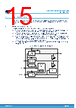
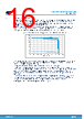
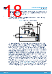
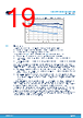
18 / 56 page  In case of UVLO condition (VDD falls below the VDD(off) threshold), the drivers turn off all the external MOSFETs, forcing the power stage into a safe condition. Concurrently, the nFAULT open-drain pin is forced low. As soon as the VDD voltage rises above the VDD(On) threshold, the nFAULT is released and the drivers return to an active condition, depending on the status of the digital inputs. 5.1.3 Charge pump The embedded charge pump supplies the high-side gate drivers and ensures an unlimited on-time of the high- side MOSFETs and a PWM duty cycle of 100%. Figure 9. Charge pump simplified block diagram CFLY CBOOT UVLO Control Feedback VS VM VBOOT NCAP PCAP High-side supply High-side control logic VM VS CM CSUPPLY VCC The charge pump is supplied directly by the VS pin and generates the voltage VBOOT referenced to the motor supply VM. The VBOOT is the supply of the three high-side gate drivers and it must be greater than VM to properly turn on the high-side MOSFETs. The internal feedback circuit of the charge pump tracks the value of the voltage on the VCC pin and regulates the VBOOT to be equal to 'VM + VCC'. In this way, both the low-side and the high- side MOSFETs are driven with the same VGS, thus ensuring a more balanced behavior of the power stage. The circuit on the NCAP pin charges the capacitor CFLY; the charge is then transferred to the CBOOT capacitor through the PCAP pin. The amount of charge stored in the CFLY capacitor is controlled by the internal feedback, in order to meet the target voltage on VBOOT pin. The drop between the target value of VBOOT and its actual value depends on the voltage on the VS pin and the average load current required by the high-side drivers. The drop increases for lower VS and higher current load. Figure 10 shows the charge pump output voltage with respect to the load current at Tamb = 25 °C, using the recommended values for CFLY = 220 nF and CBOOT = 1 µF. The pulsed current required by the high-side drivers is provided by the CBOOT capacitor. This capacitor should be sized according to the maximum allowed ripple and total gate charge of the external MOSFETs. A ceramic low ESR capacitor of the same value of CBOOT must be placed close to the VM pin and the exposed pad (GND) of the STDRIVE102BH/H. The high-side drivers are connected to VBOOT by an internal connection: for no reason can other external loads be connected to the VBOOT pin. The VBOOT pin is referred to the VM pin: any external event forcing a 'VBOOT - VM' voltage below the limit reported in Table 1. Absolute maximum ratings, results in the device breakdown. In case of undervoltage ('VBOOT - VM ' < VCPump(Off)), the UVLO protection turns off the high-side MOSFETs, while the low-side drivers keep on operating. The high-side drivers return operative when 'VBOOT - VM' > VCPump(On). STDRIVE102BH, STDRIVE102H Device description DS14545 - Rev 1 page 18/56 |
|
链接网址 |
| ALLDATASHEET是否为您带来帮助? [ DONATE ] |
关于 Alldatasheet | 广告服务 | 联系我们 | 隐私政策 | 数据表链接 | 链接交换 | 制造商名单 All Rights Reserved©Alldatasheet.com |
| Russian : Alldatasheetru.com | Korean : Alldatasheet.co.kr | Spanish : Alldatasheet.es | French : Alldatasheet.fr | Italian : Alldatasheetit.com Portuguese : Alldatasheetpt.com | Polish : Alldatasheet.pl | Vietnamese : Alldatasheet.vn Indian : Alldatasheet.in | Mexican : Alldatasheet.com.mx | British : Alldatasheet.co.uk | New Zealand : Alldatasheet.co.nz |
|
Family Site : ic2ic.com |
icmetro.com |
 Chinese ▼
 English
 Chinese
 German
 Japanese
 Russian
 Korean
 Spanish
 French
 Italian
 Portuguese
 Polish
 Vietnamese
 Indian
 Mexican
 British
 New Zealand