|
数据搜索系统,热门电子元器件搜索 |
|
|
数据搜索系统,热门电子元器件搜索 |
|
AD8510ARM-R2 数据表(PDF) 13 Page - Analog Devices |
|
|
|||||||||||||||||||||||||||||
AD8510ARM-R2 数据表(HTML) 13 Page - Analog Devices |
|
|
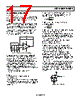
13 / 20 page  AD8510/AD8512/AD8513 Rev. H | Page 13 of 20 GENERAL APPLICATION INFORMATION INPUT OVERVOLTAGE PROTECTION The AD8510/AD8512/AD8513 have internal protective circuitry that allows voltages as high as 0.7 V beyond the supplies to be applied at the input of either terminal without causing damage. For higher input voltages, a series resistor is necessary to limit the input current. The resistor value can be determined from the formula mA 5 ≤ − S S IN R V V With a very low offset current of <0.5 nA up to 125°C, higher resistor values can be used in series with the inputs. A 5 kΩ resistor protects the inputs from voltages as high as 25 V beyond the supplies and adds less than 10 μV to the offset. OUTPUT PHASE REVERSAL Phase reversal is a change of polarity in the transfer function of the amplifier. This can occur when the voltage applied at the input of an amplifier exceeds the maximum common-mode voltage. Phase reversal can cause permanent damage to the device and can result in system lockups. The AD8510/AD8512/AD8513 do not exhibit phase reversal when input voltages are beyond the supplies. TIME (20µs/DIV) VIN VOUT VSY = ±5V AV = 1 RL = 10kΩ Figure 41. No Phase Reversal TOTAL HARMONIC DISTORTION (THD) + NOISE The AD8510/AD8512/AD8513 have low THD and excellent gain linearity, making these amplifiers great choices for precision circuits with high closed-loop gain and for audio application circuits. Figure 42 shows that the AD8510/AD8512/AD8513 have approximately 0.0005% of total distortion when configured in positive unity gain (the worst case) and driving a 100 kΩ load. FREQUENCY (Hz) 0.01 0.001 0.0001 20 100 1k 10k 20k VSY = ±5V RL = 100kΩ BW = 22kHz Figure 42. THD + N vs. Frequency TOTAL NOISE INCLUDING SOURCE RESISTORS The low input current noise and input bias current of the AD8510/AD8512/AD8513 make them the ideal amplifiers for circuits with substantial input source resistance. Input offset voltage increases by less than 15 nV per 500 Ω of source resistance at room temperature. The total noise density of the circuit is ( ) S S n n nTOTAL kTR R i e e 4 2 2 + + = where: en is the input voltage noise density of the parts. in is the input current noise density of the parts. RS is the source resistance at the noninverting terminal. k is Boltzmann’s constant (1.38 × 10⁻²³ J/K). T is the ambient temperature in Kelvin (T = 273 + °C). For RS < 3.9 kΩ, en dominates and enTOTAL ≈ en. The current noise of the AD8510/AD8512/AD8513 is so low that its total density does not become a significant term unless RS is greater than 165 MΩ, an impractical value for most applications. The total equivalent rms noise over a specific bandwidth is expressed as BW e e nTOTAL nTOTAL = where BW is the bandwidth in hertz. Note that the previous analysis is valid for frequencies larger than 150 Hz and assumes flat noise above 10 kHz. For lower frequencies, flicker noise (1/f) must be considered. |
|
|
链接网址 |
| ALLDATASHEET是否为您带来帮助? [ DONATE ] |
关于 Alldatasheet | 广告服务 | 联系我们 | 隐私政策 | 数据表链接 | 链接交换 | 制造商名单 All Rights Reserved©Alldatasheet.com |
| Russian : Alldatasheetru.com | Korean : Alldatasheet.co.kr | Spanish : Alldatasheet.es | French : Alldatasheet.fr | Italian : Alldatasheetit.com Portuguese : Alldatasheetpt.com | Polish : Alldatasheet.pl | Vietnamese : Alldatasheet.vn Indian : Alldatasheet.in | Mexican : Alldatasheet.com.mx | British : Alldatasheet.co.uk | New Zealand : Alldatasheet.co.nz |
|
Family Site : ic2ic.com |
icmetro.com |
 Chinese ▼
 English
 Chinese
 German
 Japanese
 Russian
 Korean
 Spanish
 French
 Italian
 Portuguese
 Polish
 Vietnamese
 Indian
 Mexican
 British
 New Zealand