|
数据搜索系统,热门电子元器件搜索 |
|
|
数据搜索系统,热门电子元器件搜索 |
|
AD8510ARM-R2 数据表(PDF) 18 Page - Analog Devices |
|
|
|||||||||||||||||||||||||||||
AD8510ARM-R2 数据表(HTML) 18 Page - Analog Devices |
|
|
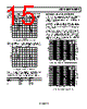
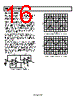
18 / 20 page  AD8510/AD8512/AD8513 Rev. H | Page 18 of 20 TIME (2ms/DIV) The AD8510 single has two additional active terminals that are not present on the AD8512 dual or AD8513 quad parts. These pins are labeled “null” and are used for fine adjustment of the input offset voltage. Although the guaranteed maximum offset voltage at room temperature is 400 μV and over the −40°C to +125°C range is 800 mV maximum, this offset voltage can be reduced by adding a potentiometer to the null pins as shown in Figure 58. With the 20 kΩ potentiometer shown, the adjustment range is approximately ±3.5 mV. The potentiometer parallels low value resistors in the drain circuit of the JFET differential input pair and allows unbalancing of the drain currents to change the offset voltage. If offset adjustment is not required, these pins should be left unconnected. Caution should be used when adding adjusting potentiometers to any op amp with this capability for several reasons. First, there is gain from these nodes to the output; therefore, capacitive coupling from noisy traces to these nodes will inject noise into the signal path. Second, the temperature coefficient of the potentiometer will not match the temperature coefficient of the internal resistors, so the offset voltage drift with temperature will be slightly affected. Third, this provision is for adjusting the offset voltage of the op amp, not for adjusting the offset of the overall system. Although it is tempting to decrease the value of the potentiometer to attain more range, this will adversely affect the dc and ac parameters. Instead, increase the potentiometer to 50 kΩ to decrease the range if needed. Figure 55. Pulse-Width Modulation Crosstalk Crosstalk, also known as channel separation, is a measure of signal feedthrough from one channel to another on the same IC. The AD8512/AD8513 have a channel separation of better than −90 dB for frequencies up to 10 kHz and of better than −50 dB for frequencies up to 10 MHz. Figure 57 shows the typical channel separation behavior between Amplifier A (driving amplifier) and each of the following: Amplifier B, Amplifier C, and Amplifier D. VOUT 1 2 7 6 5 4 3 8 +VS 20kΩ 2.2kΩ 5kΩ 5kΩ –VS VIN 18V p-p CROSSTALK = 20 log VOUT 10VIN 1 5 4 7 3 6 2 AD8510 INPUT OUTPUT V+ VOS TRIM RANGE IS TYPICALLY ±3.5mV 20kΩ V– – + Figure 56. Crosstalk Test Circuit FREQUENCY (Hz) 100 –160 10k –140 –120 –80 1k –60 –20 –40 100k 1M 10M –100 0 CH D CH C CH B Figure 58. Optional Offset Nulling Circuit Figure 57. Channel Separation |
|
|
链接网址 |
| ALLDATASHEET是否为您带来帮助? [ DONATE ] |
关于 Alldatasheet | 广告服务 | 联系我们 | 隐私政策 | 数据表链接 | 链接交换 | 制造商名单 All Rights Reserved©Alldatasheet.com |
| Russian : Alldatasheetru.com | Korean : Alldatasheet.co.kr | Spanish : Alldatasheet.es | French : Alldatasheet.fr | Italian : Alldatasheetit.com Portuguese : Alldatasheetpt.com | Polish : Alldatasheet.pl | Vietnamese : Alldatasheet.vn Indian : Alldatasheet.in | Mexican : Alldatasheet.com.mx | British : Alldatasheet.co.uk | New Zealand : Alldatasheet.co.nz |
|
Family Site : ic2ic.com |
icmetro.com |
 Chinese ▼
 English
 Chinese
 German
 Japanese
 Russian
 Korean
 Spanish
 French
 Italian
 Portuguese
 Polish
 Vietnamese
 Indian
 Mexican
 British
 New Zealand