|
数据搜索系统,热门电子元器件搜索 |
|
|
数据搜索系统,热门电子元器件搜索 |
|
AD8510ARM-R2 数据表(PDF) 17 Page - Analog Devices |
|
|
|||||||||||||||||||||||||||||
AD8510ARM-R2 数据表(HTML) 17 Page - Analog Devices |
|
|
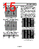
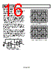
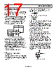
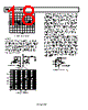
17 / 20 page  AD8510/AD8512/AD8513 Rev. H | Page 17 of 20 I-V CONVERSION APPLICATIONS Photodiode Circuits Common applications for I-V conversion include photodiode circuits where the amplifier is used to convert a current emitted by a diode placed at the positive input terminal into an output voltage. The AD8510/AD8512/AD8513’s low input bias current, wide bandwidth, and low noise make them each an excellent choice for various photodiode applications, including fax machines, fiber optic controls, motion sensors, and bar code readers. The circuit shown in Figure 53 uses a silicon diode with zero bias voltage. This is known as a photovoltaic mode; this configuration limits the overall noise and is suitable for instrumentation applications. 4 7 3 6 2 AD8510 Cf R2 Rd Ct VEE VCC Figure 53. Equivalent Preamplifier Photodiode Circuit A larger signal bandwidth can be attained at the expense of additional output noise. The total input capacitance (Ct) consists of the sum of the diode capacitance (typically 3 pF to 4 pF) and the amplifier’s input capacitance (12 pF), which includes external parasitic capacitance. Ct creates a pole in the frequency response that can lead to an unstable system. To ensure stability and optimize the bandwidth of the signal, a capacitor is placed in the feedback loop of the circuit shown in Figure 53. It creates a zero and yields a bandwidth whose corner frequency is 1/(2π(R2Cf)). The value of R2 can be determined by the ratio V /ID where: V is the desired output voltage of the op amp. ID is the diode current. For example, if ID is 100 μA and a 10 V output voltage is desired, R2 should be 100 kΩ. Rd (see Figure 53) is a junction resistance that drops typically by a factor of 2 for every 10°C increase in temperature. A typical value for Rd is 1000 MΩ. Because Rd >> R2, the circuit behavior is not impacted by the effect of the junction resistance. The maximum signal bandwidth is Ct R ft f MAX 2 2π = where ft is the unity gain frequency of the amplifier. Cf can be calculated by ft R Ct Cf 2 2π = where ft is the unity gain frequency of the op amp, and it achieves a phase margin, φM, of approximately 45°. A higher phase margin can be obtained by increasing the value of Cf. Setting Cf to twice the previous value yields approximately φM = 65° and a maximal flat frequency response, but it reduces the maximum signal bandwidth by 50%. Using the previous parameters with a Cf ≈ 1 pF, the signal bandwidth is approximately 2.6 MHz. Signal Transmission Applications One popular signal transmission method uses pulse-width modulation. High data rates may require a fast comparator rather than an op amp. However, the need for sharp, undistorted signals may favor using a linear amplifier. The AD8510/AD8512/AD8513 make excellent voltage comparators. In addition to a high slew rate, the AD8510/ AD8512/AD8513 have a very fast saturation recovery time. In the absence of feedback, the amplifiers are in open-loop mode (very high gain). In this mode of operation, they spend much of their time in saturation. The circuit shown in Figure 54 was used to compare two signals of different frequencies, namely a 100 Hz sine wave and a 1 kHz triangular wave. Figure 55 shows a scope plot of the resulting output waveforms. A pull-up resistor (typically 5 kΩ) can be connected from the output to VCC if the output voltage needs to reach the positive rail. The trade-off is that power consumption is higher. VOUT V1 V2 4 2 6 7 3 –15V +15V Figure 54. Pulse-Width Modulator |
|
|
链接网址 |
| ALLDATASHEET是否为您带来帮助? [ DONATE ] |
关于 Alldatasheet | 广告服务 | 联系我们 | 隐私政策 | 数据表链接 | 链接交换 | 制造商名单 All Rights Reserved©Alldatasheet.com |
| Russian : Alldatasheetru.com | Korean : Alldatasheet.co.kr | Spanish : Alldatasheet.es | French : Alldatasheet.fr | Italian : Alldatasheetit.com Portuguese : Alldatasheetpt.com | Polish : Alldatasheet.pl | Vietnamese : Alldatasheet.vn Indian : Alldatasheet.in | Mexican : Alldatasheet.com.mx | British : Alldatasheet.co.uk | New Zealand : Alldatasheet.co.nz |
|
Family Site : ic2ic.com |
icmetro.com |
 Chinese ▼
 English
 Chinese
 German
 Japanese
 Russian
 Korean
 Spanish
 French
 Italian
 Portuguese
 Polish
 Vietnamese
 Indian
 Mexican
 British
 New Zealand