|
数据搜索系统,热门电子元器件搜索 |
|
|
数据搜索系统,热门电子元器件搜索 |
|
AD8532ARM-R2 数据表(PDF) 13 Page - Analog Devices |
|
|
|||||||||||||||||||||||||||||
AD8532ARM-R2 数据表(HTML) 13 Page - Analog Devices |
|
|
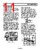
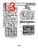
13 / 20 page  AD8531/AD8532/AD8534 Rev. F | Page 13 of 20 5V RS 5Ω CS 1µF VOUT VIN 100mV p-p AD8532 CL 47nF OUTPUT PHASE REVERSAL Some operational amplifiers designed for single-supply operation exhibit an output voltage phase reversal when their inputs are driven beyond their useful common-mode range. The AD8531/ AD8532/AD8534 are free from reasonable input voltage range restrictions, provided that input voltages no greater than the supply voltage rails are applied. Although the output of the device does not change phase, large currents can flow through internal junctions to the supply rails, which was described in the Input Overvoltage Protection section. Without limit, these fault currents can easily destroy the amplifier. The technique recommended in the Input Overvoltage Protection section should therefore be applied in those applications where the possibility of input voltages exceeding the supply voltages exists. Figure 40. Snubber Network Compensates for Capacitive Loads The first step is to determine the value of the resistor, RS. A good starting value is 100 Ω. This value is reduced until the small signal transient response is optimized. Next, CS is determined; 10 μF is a good starting point. This value is reduced to the smallest value for acceptable performance (typically, 1 μF). For the case of a 47 nF load capacitor on the AD8531/AD8532/AD8534, the optimal snubber network is 5 Ω in series with 1 μF. The benefit is immediately apparent, as seen in Figure 41. The top trace was taken with a 47 nF load, and the bottom trace was taken with the 5 Ω in series with a 1 μF snubber network in place. The amount of overshoot and ringing is dramatically reduced. Table 5 illustrates a few sample snubber networks for large load capacitors. CAPACITIVE LOAD DRIVE The AD8531/AD8532/AD8534 exhibit excellent capacitive load driving capabilities. They can drive up to 10 nF directly, as shown in Figure 25 through Figure 28. However, even though the device is stable, a capacitive load does not come without a penalty in bandwidth. As shown in Figure 39, the bandwidth is reduced to less than 1 MHz for loads greater than 10 nF. A snubber network on the output does not increase the bandwidth, but it does significantly reduce the amount of overshoot for a given capacitive load. A snubber consists of a series RC network (RS, CS), as shown in Figure 40, connected from the output of the device to ground. This network operates in parallel with the load capacitor, CL, to provide phase lag compensation. The actual value of the resistor and capacitor is best determined empirically. Table 5. Snubber Networks for Large Capacitive Loads Load Capacitance (CL) Snubber Network (RS, CS) 0.47 nF 300 Ω, 0.1 μF 4.7 nF 30 Ω, 1 μF 47 nF 5 Ω, 1 μF 10 0% 100 47nF LOAD ONLY SNUBBER IN CIRCUIT 90 10µs 50mV 50mV CAPACITIVE LOAD (nF) 3.5 4.0 3.0 2.5 2.0 1.5 1.0 0.5 0 0.01 0.1 1 10 100 VS = ±2.5V RL = 1kΩ TA = 25°C Figure 41. Overshoot and Ringing Are Reduced by Adding a Snubber Network in Parallel with the 47 nF Load Figure 39. Unity-Gain Bandwidth vs. Capacitive Load |
|
|
链接网址 |
| ALLDATASHEET是否为您带来帮助? [ DONATE ] |
关于 Alldatasheet | 广告服务 | 联系我们 | 隐私政策 | 数据表链接 | 链接交换 | 制造商名单 All Rights Reserved©Alldatasheet.com |
| Russian : Alldatasheetru.com | Korean : Alldatasheet.co.kr | Spanish : Alldatasheet.es | French : Alldatasheet.fr | Italian : Alldatasheetit.com Portuguese : Alldatasheetpt.com | Polish : Alldatasheet.pl | Vietnamese : Alldatasheet.vn Indian : Alldatasheet.in | Mexican : Alldatasheet.com.mx | British : Alldatasheet.co.uk | New Zealand : Alldatasheet.co.nz |
|
Family Site : ic2ic.com |
icmetro.com |
 Chinese ▼
 English
 Chinese
 German
 Japanese
 Russian
 Korean
 Spanish
 French
 Italian
 Portuguese
 Polish
 Vietnamese
 Indian
 Mexican
 British
 New Zealand