|
数据搜索系统,热门电子元器件搜索 |
|
|
数据搜索系统,热门电子元器件搜索 |
|
AD8532ARM-R2 数据表(PDF) 14 Page - Analog Devices |
|
|
|||||||||||||||||||||||||||||
AD8532ARM-R2 数据表(HTML) 14 Page - Analog Devices |
|
|
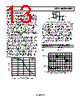
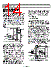
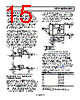
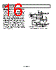
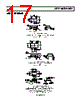
14 / 20 page  AD8531/AD8532/AD8534 Rev. F | Page 14 of 20 APPLICATIONS INFORMATION HIGH OUTPUT CURRENT, BUFFERED REFERENCE/REGULATOR Many applications require stable voltage outputs relatively close in potential to an unregulated input source. This low dropout type of reference/regulator is readily implemented with a rail- to-rail output op amp and is particularly useful when using a higher current device, such as the AD8531/AD8532/AD8534. A typical example is the 3.3 V or 4.5 V reference voltage developed from a 5 V system source. Generating these voltages requires a three terminal reference, such as the REF196 (3.3 V) or the REF194 (4.5 V), both of which feature low power, with sourcing outputs of 30 mA or less. Figure 42 shows how such a reference can be outfitted with an AD8531/AD8532/AD8534 buffer for higher currents and/or voltage levels, plus sink and source load capability. R2 10kΩ 1% VOUT1 = 3.3V @ 100mA R5 0.2Ω C5 100µF/16V TANTALUM R1 10kΩ 1% C1 0.1µF VS 5V VOUT2 = 3.3V C4 1µF 6 2 3 4 VOUT COMMON C3 0.1µF C2 0.1µF VC ON/OFF CONTROL INPUT CMOS HI (OR OPEN) = ON LO = OFF VS COMMON R3 (See Text) R4 3.3kΩ U2 AD8531 U1 REF196 Figure 42. High Output Current Reference/Regulator The low dropout performance of this circuit is provided by stage U2, an AD8531 connected as a follower/buffer for the basic reference voltage produced by U1. The low voltage saturation characteristic of the AD8531/AD8532/AD8534 allows up to 100 mA of load current in the illustrated use, as a 5 V to 3.3 V converter with good dc accuracy. In fact, the dc output voltage change for a 100 mA load current delta measures less than 1 mV. This corresponds to an equivalent output impedance of < 0.01 Ω. In this application, the stable 3.3 V from U1 is applied to U2 through a noise filter, R1 to C1. U2 replicates the U1 voltage within a few millivolts, but at a higher current output at VOUT1, with the ability to both sink and source output current(s), unlike most IC references. R2 and C2 in the feedback path of U2 provide additional noise filtering. Transient performance of the reference/regulator for a 100 mA step change in load current is also quite good and is largely determined by the R5 to C5 output network. With values as shown, the transient is about 20 mV peak and settles to within 2 mV in less than 10 μs for either polarity. Although room exists for optimizing the transient response, any changes to the R5 to C5 network should be verified by experiment to preclude the possibility of excessive ringing with some capacitor types. To scale VOUT2 to another (higher) output level, the optional resistor R3 (shown dotted in Figure 42) is added, causing the new VOUT1 to become ⎟ ⎠ ⎞ ⎜ ⎝ ⎛ + × = R3 R2 V V OUT2 OUT1 1 The circuit can either be used as shown, as a 5 V to 3.3 V reference/regulator, or with on/off control. By driving Pin 3 of U1 with a logic control signal as noted, the output is switched on/off. Note that when on/off control is used, R4 must be used with U1 to speed on/off switching. SINGLE-SUPPLY, BALANCED LINE DRIVER The circuit in Figure 43 is a unique line driver circuit topology used in professional audio applications. It was modified for automotive and multimedia audio applications. On a single 5 V supply, the line driver exhibits less than 0.7% distortion into a 600 Ω load from 20 Hz to 15 kHz (not shown) with an input signal level of 4 V p-p. In fact, the output drive capability of the AD8531/AD8532/AD8534 maintains this level for loads as small as 32 Ω. For input signals less than 1 V p-p, the THD is less than 0.1%, regardless of load. The design is a transformer- less, balanced transmission system where output common- mode rejection of noise is of paramount importance. As with the transformer-based system, either output can be shorted to ground for unbalanced line driver applications without changing the circuit gain of 1. Other circuit gains can be set according to the equation in the diagram. This allows the design to be easily configured for inverting, noninverting, or differential operation. RL 600Ω C1 22µF A2 7 6 5 3 1 2 A1 5V R1 10kΩ R2 10kΩ R11 10kΩ R7 10kΩ 6 7 5 A1 12V 5V R8 100kΩ R9 100kΩ C2 1µF R12 10kΩ R14 50Ω A2 1 2 3 R3 10kΩ R6 10kΩ R13 10kΩ C3 47µF VOUT1 VOUT2 C4 47µF A1, A2 = 1/2 AD8532 GAIN = R3 R2 SET: R7, R10, R11 = R2 SET: R6, R12, R13 = R3 VIN R10 10kΩ R5 50Ω Figure 43. Single-Supply, Balanced Line Driver for Multimedia and Automotive Applications |
|
|
链接网址 |
| ALLDATASHEET是否为您带来帮助? [ DONATE ] |
关于 Alldatasheet | 广告服务 | 联系我们 | 隐私政策 | 数据表链接 | 链接交换 | 制造商名单 All Rights Reserved©Alldatasheet.com |
| Russian : Alldatasheetru.com | Korean : Alldatasheet.co.kr | Spanish : Alldatasheet.es | French : Alldatasheet.fr | Italian : Alldatasheetit.com Portuguese : Alldatasheetpt.com | Polish : Alldatasheet.pl | Vietnamese : Alldatasheet.vn Indian : Alldatasheet.in | Mexican : Alldatasheet.com.mx | British : Alldatasheet.co.uk | New Zealand : Alldatasheet.co.nz |
|
Family Site : ic2ic.com |
icmetro.com |
 Chinese ▼
 English
 Chinese
 German
 Japanese
 Russian
 Korean
 Spanish
 French
 Italian
 Portuguese
 Polish
 Vietnamese
 Indian
 Mexican
 British
 New Zealand