|
数据搜索系统,热门电子元器件搜索 |
|
|
数据搜索系统,热门电子元器件搜索 |
|
TNETA1585 数据表(PDF) 6 Page - Texas Instruments |
|
|
|||||||||||||||||||||||||||||
TNETA1585 数据表(HTML) 6 Page - Texas Instruments |
|
|
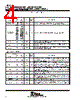
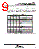
6 / 32 page  TNETA1585 ATM TRAFFIC MANAGEMENT SCHEDULER DEVICE WITH RECEIVE UTOPIA AND COPROCESSOR INTERFACES SDNS041A – NOVEMBER 1996 – REVISED JULY 1998 6 POST OFFICE BOX 655303 • DALLAS, TEXAS 75265 Terminal Functions (Continued) boundary-scan interface TERMINAL RESET NAME NO. PGF NO. PCM I/O RESET STATE DESCRIPTION TCK 4 4 I (TTL) I Test clock. TCK is used to clock the test-access-port (TAP) operation. TDI 1 1 I (TTL) I Test data input. TDI is used to shift serial test data and instruction into the device during TAP operation. TDO 2 2 O (CMOS) Hi-Z Test data output. TDO is used to shift serial test data and instructions out of the device during TAP operation. TMS 3 3 I (TTL) I Test mode select. TMS is used to control the state of the TAP controller. TRST 6 6 I (TTL) I Test reset. TRST asynchronously forces the TAP controller to a known state. miscellaneous signals TERMINAL RESET NAME NO. PGF NO. PCM I/O RESET STATE DESCRIPTION CONFIG 9 9 I (TTL) I This terminal must be tied low during normal operation. TESTMODE 7 7 I (TTL) I Test/normal mode. TESTMODE selects test mode when high and normal operation when low. power and ground TERMINAL NAME NO. PGF NO. PCM DESCRIPTION GND 5, 15, 27, 40, 50, 58, 67, 77, 84, 94, 103, 112, 122, 130, 138, 147, 156, 166, 174 5, 14, 25, 36, 46, 53, 61, 69, 76, 86, 94, 102, 110, 118, 126, 134, 142, 150, 158 Ground. GND is the 0-V reference for the device. NC 13, 17, 28, 30, 32, 57, 61, 72, 76, 101, 105, 116, 120, 145, 149, 160, 164, 173, 175, 176 27, 157, 159, 160 No internal connection. NC terminals have no internal connections. For potential functionality additions, it is recommended that these terminals not be connected to any signal, power, or ground connection. VCC 11, 37, 46, 63, 71, 90, 98, 117, 126, 142, 152, 161, 170 11, 33, 42, 57, 65, 82, 90, 106, 114, 130, 138, 146, 154 Supply voltage. VCC is the 3.3-V (with respect to GND) supply for the functional logic gates. VCC(5V) 8, 21, 54, 80, 108, 134 8, 19, 50, 72, 98, 122 Supply voltage. VCC(5 V) is the 5-V secondary supply voltage for the clamp diodes of 5-V tolerant input and output buffers. The clamp diodes provide protection for the buffers in a 5-V switching environment. |
|
链接网址 |
| ALLDATASHEET是否为您带来帮助? [ DONATE ] |
关于 Alldatasheet | 广告服务 | 联系我们 | 隐私政策 | 数据表链接 | 链接交换 | 制造商名单 All Rights Reserved©Alldatasheet.com |
| Russian : Alldatasheetru.com | Korean : Alldatasheet.co.kr | Spanish : Alldatasheet.es | French : Alldatasheet.fr | Italian : Alldatasheetit.com Portuguese : Alldatasheetpt.com | Polish : Alldatasheet.pl | Vietnamese : Alldatasheet.vn Indian : Alldatasheet.in | Mexican : Alldatasheet.com.mx | British : Alldatasheet.co.uk | New Zealand : Alldatasheet.co.nz |
|
Family Site : ic2ic.com |
icmetro.com |
 Chinese ▼
 English
 Chinese
 German
 Japanese
 Russian
 Korean
 Spanish
 French
 Italian
 Portuguese
 Polish
 Vietnamese
 Indian
 Mexican
 British
 New Zealand