|
数据搜索系统,热门电子元器件搜索 |
|
|
数据搜索系统,热门电子元器件搜索 |
|
ADRF6806ACPZ-R7 数据表(PDF) 17 Page - Analog Devices |
|
|
|||||||||||||||||||||||||||||
ADRF6806ACPZ-R7 数据表(HTML) 17 Page - Analog Devices |
|
|
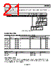
17 / 36 page  Data Sheet ADRF6806 Rev. B | Page 17 of 36 Register 4—Charge Pump, PFD, and Reference Path Control With R4[2:0] set to 100, the on-chip charge pump, PFD, and reference path control register is programmed as shown in Figure 37. The charge pump current is controlled by the base charge pump current (ICP, BASE), and the value of the charge pump current multiplier (ICP, MULT). The base charge pump current can be set using an internal or external resistor (according to DB18 of Register 4). When using an external resistor, the value of ICP,BASE can be varied according to [] 8 . 37 250 4 . 217 Ω , − ⎥⎦ ⎤ ⎢⎣ ⎡ × = BASE CP SET I R The actual charge pump current can be programmed to be a multiple (1, 2, 3, or 4) of the charge pump base current. The multiplying value (ICP, MULT) is equal to 1 plus the value of the DB11 and DB10 bits in Register 4. The PFD phase offset multiplier (θPFD, OFS), which is set by Bit DB16 to Bit DB12 of Register 4, causes the PLL to lock with a nominally fixed phase offset between the PFD reference signal and the divided-down VCO signal. This phase offset is used to linearize the PFD-CP transfer function and can improve fractional spurs. The magnitude of the phase offset is determined by MULT CP OFS PFD I , , 5 . 22 [deg] ΔΦ θ = Finally, the phase offset can be either positive or negative depending on the value of the DB17 bit in Register 4. The reference frequency applied to the PFD can be manipulated using the internal reference path source. The external reference frequency applied can be internally scaled in frequency by 2×, 1×, 0.5×, or 0.25×. This allows a broader range of reference frequency selections while keeping the reference frequency applied to the PFD within an acceptable range. The ADRF6801 also provides a MUXOUT pin that can be programmed to output a selection of several internal signals. The default mode provides a lock-detect output that allows users to verify when the PLL has locked to the target frequency. In addition, several other internal signals can be routed to the MUXOUT pin as described in Figure 37. |
|
链接网址 |
| ALLDATASHEET是否为您带来帮助? [ DONATE ] |
关于 Alldatasheet | 广告服务 | 联系我们 | 隐私政策 | 数据表链接 | 链接交换 | 制造商名单 All Rights Reserved©Alldatasheet.com |
| Russian : Alldatasheetru.com | Korean : Alldatasheet.co.kr | Spanish : Alldatasheet.es | French : Alldatasheet.fr | Italian : Alldatasheetit.com Portuguese : Alldatasheetpt.com | Polish : Alldatasheet.pl | Vietnamese : Alldatasheet.vn Indian : Alldatasheet.in | Mexican : Alldatasheet.com.mx | British : Alldatasheet.co.uk | New Zealand : Alldatasheet.co.nz |
|
Family Site : ic2ic.com |
icmetro.com |
 Chinese ▼
 English
 Chinese
 German
 Japanese
 Russian
 Korean
 Spanish
 French
 Italian
 Portuguese
 Polish
 Vietnamese
 Indian
 Mexican
 British
 New Zealand