|
数据搜索系统,热门电子元器件搜索 |
|
|
数据搜索系统,热门电子元器件搜索 |
|
AD8351ARM-R2 数据表(PDF) 10 Page - Analog Devices |
|
|
|||||||||||||||||||||||||||||
AD8351ARM-R2 数据表(HTML) 10 Page - Analog Devices |
|
|
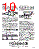
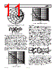
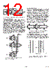
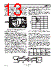
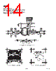
10 / 16 page  REV. B –10– AD8351 BASIC CONCEPTS Differential signaling is used in high performance signal chains, where distortion performance, signal-to-noise ratio, and low power consumption is critical. Differential circuits inherently provide improved common-mode rejection and harmonic distortion perfor- mance as well as better immunity to interference and ground noise. VOCM 10 VPOS 9 OPHI 8 OPLO 7 COMM 6 1 PWUP RGP1 2 INHI 3 INLO 4 RGP2 5 RG BALANCED SOURCE RL A A 2A Figure 1. Differential Circuit Representation Figure 1 illustrates the expected input and output waveforms for a typical application. Usually the applied input waveform will be a balanced differential drive, where the signal applied to the INHI and INLO pins are equal in amplitude and differ in phase by 180 °. In some applications, baluns may be used to transform a single- ended drive signal to a differential signal. The AD8351 may also be used to transform a single-ended signal to a differential signal. GAIN ADJUSTMENT The differential gain of the AD8351 is set using a single external resistor, RG, which is connected between Pins 2 and 5. The gain can be set to any value between 0 dB and 26 dB using the resistor values specified in TPC 2, with common gain values provided in Table I. The board traces used to connect the external gain resis- tor should be balanced and as short as possible to help prevent noise pickup and to ensure balanced gain and stability. The low frequency voltage gain of the AD8351 can be modeled as A RR R R RR R R R R V V V LG F L GL G L F G OUT IN = × () +× × ×× + × + + ()×+ () = 56 92 46 19 539 .. .. where: RF is 350 Ω (internal). RL is the single-ended load resistance. RG is the gain setting resistor. Table I. Gain Resistor Selection for Common Gain Values (Load Resistance Is Specified as Single-Ended) Gain, AV RG (RL = 75 )RG (RL = 500 ) 0 dB 680 Ω 2 k Ω 6 dB 200 Ω 470 Ω 10 dB 100 Ω 200 Ω 20 dB 22 Ω 43 Ω COMMON-MODE ADJUSTMENT The output common-mode voltage level is the dc offset voltage present at each of the differential outputs. The ac signals are of equal amplitude with a 180 ° phase difference but are centered at the same common-mode voltage level. The common-mode output voltage level can be adjusted from 1.2 V to 3.8 V by driving the desired voltage level into the VOCM pin, as illus- trated in Figure 2. VOCM 10 VPOS 9 OPHI 8 OPLO 7 COMM 6 1 PWUP RGP1 2 INHI 3 INLO 4 RGP2 5 RG BALANCED SOURCE RL 0.1 F VS VOCM 1.2V TO 3.8V CDECL 0.1 F Figure 2. Common-Mode Adjustment INPUT AND OUTPUT MATCHING The AD8351 provides a moderately high differential input impedance of 5 k Ω. In practical applications, the input of the AD8351 will be terminated to a lower impedance to provide an impedance match to the driving source, as depicted in Figure 3. The terminating resistor, RT, should be as close as possible to the input pins in order to minimize reflections due to imped- ance mismatch. The 150 Ω output impedance may need to be transformed to provide the desired output match to a given load. Matching components can be calculated using a Smith Chart or by using a resonant approach to determine the match- ing network that results in a complex conjugate match. The input and output impedances and reflection coefficients are provided in TPCs 19, 20, 22, and 23. For additional informa- tion on reactive matching to differential sources and loads, refer to the Applications section of the AD8350 data sheet. Figure 3 illustrates a SAW (surface acoustic wave) filter inter- face. Many SAW filters are inherently differential, allowing for a low loss output match. In this example, the SAW filter requires a 50 Ω source impedance in order to provide the desired center frequency and Q. The series L shunt C output network provides a 150 Ω to 50 Ω impedance transformation at the desired frequency of operation. The impedance transformation is illustrated on a Smith Chart in Figure 4. It is possible to drive a single-ended SAW filter simply by con- necting the unused output to ground using the appropriate terminating resistance. The overall gain of the system will be reduced by 6 dB due to the fact that only half of the signal will be available to the input of the SAW filter. BALANCED SOURCE RS RS RS = RT RT RT 0.1 F 0.1 F RG 0.1 F 0.1 F 150 CP 8pF LS 27nF LS 27nF 50 190MHz SAW VPOS AD8351 Figure 3. Example of Differential SAW Filter Interface (fC = 190 MHz) |
|
|
链接网址 |
| ALLDATASHEET是否为您带来帮助? [ DONATE ] |
关于 Alldatasheet | 广告服务 | 联系我们 | 隐私政策 | 数据表链接 | 链接交换 | 制造商名单 All Rights Reserved©Alldatasheet.com |
| Russian : Alldatasheetru.com | Korean : Alldatasheet.co.kr | Spanish : Alldatasheet.es | French : Alldatasheet.fr | Italian : Alldatasheetit.com Portuguese : Alldatasheetpt.com | Polish : Alldatasheet.pl | Vietnamese : Alldatasheet.vn Indian : Alldatasheet.in | Mexican : Alldatasheet.com.mx | British : Alldatasheet.co.uk | New Zealand : Alldatasheet.co.nz |
|
Family Site : ic2ic.com |
icmetro.com |
 Chinese ▼
 English
 Chinese
 German
 Japanese
 Russian
 Korean
 Spanish
 French
 Italian
 Portuguese
 Polish
 Vietnamese
 Indian
 Mexican
 British
 New Zealand