|
数据搜索系统,热门电子元器件搜索 |
|
|
数据搜索系统,热门电子元器件搜索 |
|
AD8351ARM-R2 数据表(PDF) 11 Page - Analog Devices |
|
|
|||||||||||||||||||||||||||||
AD8351ARM-R2 数据表(HTML) 11 Page - Analog Devices |
|
|
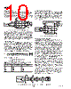
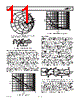
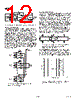
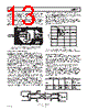
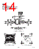
11 / 16 page  REV. B AD8351 –11– 200 0 50 150 SERIES L SHUNT C 500 100 50 25 10 200 100 500 50 25 10 Figure 4. Smith Chart Representation of SAW Filter Output Matching Network 50 50 AD8351 RG 0.1 F 25 RF 0.1 F 0.1 F RL 0.1 F Figure 5. Single-Ended Application SINGLE-ENDED-TO-DIFFERENTIAL OPERATION The AD8351 can easily be configured as a single-ended-to- differential gain block, as illustrated in Figure 5. The input signal is ac-coupled and applied to the INHI input. The unused input is ac-coupled to ground. The values of C1 through C4 should be selected such that their reactances are negligible at the desired frequency of operation. To balance the outputs, an external feed- back resistor, RF, is required. To select the gain resistor and the feedback resistor, refer to Figures 6a and 6b. From Figure 6a, select an RG for the required dB gain at a given load. Next, select from Figure 6b an RF resistor for the selected RG and load. Even though the differential balance is not perfect under these conditions, the distortion performance is still impressive. TPCs 10 and 11 show the second and third harmonic distortion perfor- mance when driving the input of the AD8351 using a single-ended 50 Ω source. RG ( ) 0 1000 10 0 15 5 35 20 25 30 100 RL = 500 RL = 1000 RL = 150 Figure 6a. Gain Selection RG ( ) 0 1000 2 0 3 1 7 4 5 6 100 RL = 150 RL = 1000 RL = 500 Figure 6b. Feedback Resistor Selection ADC DRIVING The circuit in Figure 7 represents a simplified front end of the AD8351 driving the AD6645, which is a 14-bit, 105 MSPS A/D converter. For optimum performance, the AD6645 and the AD8351 are driven differentially. The resistors R1 and R2 present a 50 Ω differential input impedance to the source with R3 and R4 providing isolation from the A/D input. The gain setting resistor for the AD8351 is RG. The AD6645 presents a 1 k Ω differential load to the AD8351 and requires a 2.2 V p-p differential signal between AIN and AIN for a full-scale output. This AD8351 circuit then provides the gain, isolation, and source matching for the AD6645. The AD8351 also provides a balanced input, not provided by the balun, to the AD6645, which is essential for second-order cancellation. The signal generator is bipolar, centered around ground. Connecting the VOCM pin (10) of the AD8351 to the VREF pin of the AD6645 sets the common-mode output voltage of the AD8351 at 2.4 V. This voltage is bypassed with a 0.1 µF capacitor. Increasing the gain of the AD8351 will increase the system noise and thus decrease the SNR but will not significantly affect the distortion. The circuit in Figure 7 can provide SFDR performance of better than –90 dBc with a 10 MHz input and –80 dBc with a 70 MHz input at a gain of 10 dB. BALANCE 50 SOURCE 25 100nF 25 100nF AD8351 INHI INLO RG OPHI OPLO VOCM 25 25 DIGITAL OUT AD6645 AIN AIN VREF Figure 7. ADC Driving Application Using Differential Input The circuit of Figure 8 represents a single-ended input to differ- ential output configuration of the AD8351 driving the AD6645. In this case, R1 provides the input impedance. RG is the gain setting resistor. The resistor RF is required to balance the output voltages required for second-order cancellation by the AD6645 and can be selected using a chart. (See the Single-Ended-to- Differential Operation section.) The circuit depicted in Figure 8 can provide SFDR performance of better than –90 dBc with a 10 MHz input and –77 dBc with a 70 MHz input. |
|
|
链接网址 |
| ALLDATASHEET是否为您带来帮助? [ DONATE ] |
关于 Alldatasheet | 广告服务 | 联系我们 | 隐私政策 | 数据表链接 | 链接交换 | 制造商名单 All Rights Reserved©Alldatasheet.com |
| Russian : Alldatasheetru.com | Korean : Alldatasheet.co.kr | Spanish : Alldatasheet.es | French : Alldatasheet.fr | Italian : Alldatasheetit.com Portuguese : Alldatasheetpt.com | Polish : Alldatasheet.pl | Vietnamese : Alldatasheet.vn Indian : Alldatasheet.in | Mexican : Alldatasheet.com.mx | British : Alldatasheet.co.uk | New Zealand : Alldatasheet.co.nz |
|
Family Site : ic2ic.com |
icmetro.com |
 Chinese ▼
 English
 Chinese
 German
 Japanese
 Russian
 Korean
 Spanish
 French
 Italian
 Portuguese
 Polish
 Vietnamese
 Indian
 Mexican
 British
 New Zealand