|
数据搜索系统,热门电子元器件搜索 |
|
|
数据搜索系统,热门电子元器件搜索 |
|
LTC1098AC 数据表(PDF) 15 Page - Linear Technology |
|
|
|||||||||||||||||||||||||||||
LTC1098AC 数据表(HTML) 15 Page - Linear Technology |
|
|
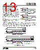
15 / 28 page  15 LTC1096/LTC1096L LTC1098/LTC1098L SGL/ DIFF ODD/ SIGN MSBF START MUX ADDRESS MSB-FIRST/ LSB-FIRST LTC1096/8 • AI02 Start Bit The first “logical one” clocked into the DIN input after CS goes low is the start bit. The start bit initiates the data transfer. The LTC1098(L) will ignore all leading zeros which precede this logical one. After the start bit is received, the remaining bits of the input word will be clocked in. Further inputs on the DIN pin are then ignored until the next CS cycle. Multiplexer (MUX) Address The bits of the input word following the START bit assign the MUX configuration for the requested conversion. For a given channel selection, the converter will measure the voltage between the two channels indicated by the “+” and “–” signs in the selected row of the followintg tables. In single-ended mode, all input channels are measured with respect to GND. MSB-First/LSB-First (MSBF) The output data of the LTC1098(L) is programmed for MSB-first or LSB-first sequence using the MSBF bit. When the MSBF bit is a logical one, data will appear on the DOUT line in MSB-first format. Logical zeros will be filled in indefinitely following the last data bit. When the MSBF bit is a logical zero, LSB-first data will follow the normal MSB-first data on the DOUT line. (see Operating Sequence) Unipolar Transfer Curve The LTC1096(L)/LTC1098(L) are permanently config- ured for unipolar only. The input span and code assign- ment for this conversion type are shown in the follow- ing figures for a 5V reference. Unipolar Transfer Curve VIN 0 0 0 0 0 0 0 1 0 0 0 0 0 0 0 0 1 1 1 1 1 1 1 1 1 1 1 1 1 1 1 0 • • • LTC1096/8 • AI04 the A/D conversion result is output on the DOUT line. Bringing CS high resets the LTC1096(L) for the next data exchange. Input Data Word The LTC1096(L) requires no DIN word. It is permanently configured to have a single differential input. The conver- sion result, in which output on the DOUT line is MSB-first sequence, followed by LSB sequence providing easy inter- face to MSB- or LSB-first serial ports. The LTC1098(L) clocks data into the DIN input on the rising edge of the clock. The input data words are defined as follows: S APPLICATI I FOR ATIO LTC1098(L) Channel Selection MUX ADDRESS SGL/DIFF 1 1 0 0 ODD/SIGN 0 1 0 1 CHANNEL # 0 + + – 1 + – + GND – – SINGLE-ENDED MUX MODE DIFFERENTIAL MUX MODE LTC1096/8 • AI03 Operation with DIN and DOUT Tied Together The LTC1098(L) can be operated with DIN and DOUT tied together. This eliminates one of the lines required to communicate to the microprocessor (MPU). Data is trans- mitted in both directions on a single wire. The processor pin connected to this data line should be configurable as either an input or an output. The LTC1098(L) will take control of the data line and drive it low on the 4th falling Unipolar Output Code OUTPUT CODE 1 1 1 1 1 1 1 1 1 1 1 1 1 1 1 0 • • • 0 0 0 0 0 0 0 1 0 0 0 0 0 0 0 0 INPUT VOLTAGE VREF – 1LSB VREF – 2LSB • • • 1LSB 0V INPUT VOLTAGE (VREF = 5.000V) 4.9805V 4.9609V • • • 0.0195V 0V LTC1096/8 • AI05 |
|
|
链接网址 |
| ALLDATASHEET是否为您带来帮助? [ DONATE ] |
关于 Alldatasheet | 广告服务 | 联系我们 | 隐私政策 | 数据表链接 | 链接交换 | 制造商名单 All Rights Reserved©Alldatasheet.com |
| Russian : Alldatasheetru.com | Korean : Alldatasheet.co.kr | Spanish : Alldatasheet.es | French : Alldatasheet.fr | Italian : Alldatasheetit.com Portuguese : Alldatasheetpt.com | Polish : Alldatasheet.pl | Vietnamese : Alldatasheet.vn Indian : Alldatasheet.in | Mexican : Alldatasheet.com.mx | British : Alldatasheet.co.uk | New Zealand : Alldatasheet.co.nz |
|
Family Site : ic2ic.com |
icmetro.com |
 Chinese ▼
 English
 Chinese
 German
 Japanese
 Russian
 Korean
 Spanish
 French
 Italian
 Portuguese
 Polish
 Vietnamese
 Indian
 Mexican
 British
 New Zealand