|
数据搜索系统,热门电子元器件搜索 |
|
|
数据搜索系统,热门电子元器件搜索 |
|
AD8510ARM-R2 数据表(PDF) 13 Page - Analog Devices |
|
|
|||||||||||||||||||||||||||||
AD8510ARM-R2 数据表(HTML) 13 Page - Analog Devices |
|
|
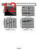
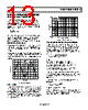
13 / 20 page  AD8510/AD8512/AD8513 Rev. E | Page 13 of 20 GENERAL APPLICATION INFORMATION INPUT OVERVOLTAGE PROTECTION The AD8510/AD8512/AD8513 have internal protective circuitry that allows voltages as high as 0.7 V beyond the supplies to be applied at the input of either terminal without causing damage. For higher input voltages, a series resistor is necessary to limit the input current. The resistor value can be determined from the formula mA R V V S S IN 5 ≤ − With a very low offset current of <0.5 nA up to 125°C, higher resistor values can be used in series with the inputs. A 5 kΩ resistor will protect the inputs to voltages as high as 25 V beyond the supplies and will add less than 10 µV to the offset. OUTPUT PHASE REVERSAL Phase reversal is a change of polarity in the transfer function of the amplifier. This can occur when the voltage applied at the input of an amplifier exceeds the maximum common-mode voltage. Phase reversal can cause permanent damage to the device and may result in system lockups. The AD8510/AD8512/AD8513 do not exhibit phase reversal when input voltages are beyond the supplies. TIME (20 µs/DIV) VIN VOUT VSY = ±5V AV = 1 RL = 10kΩ Figure 41. No Phase Reversal THD + NOISE The AD8510/AD8512/AD8513 have low total harmonic distor- tion and excellent gain linearity, making these amplifiers a great choice for precision circuits with high closed-loop gain, and for audio application circuits. Figure 42 shows that the AD8510/ AD8512/AD8513 have approximately 0.0005% of total distor- tion when configured in positive unity gain (the worst case) and driving a 100 kΩ load. FREQUENCY (Hz) 0.01 0.001 0.0001 20 100 1k 20k VSY = ±5V RL = 100kΩ BW = 22kHz Figure 42. THD + N vs. Frequency TOTAL NOISE INCLUDING SOURCE RESISTORS The low input current noise and input bias current of the AD8510/AD8512/AD8513 make them the ideal amplifiers for circuits with substantial input source resistance. Input offset voltage increases by less than 15 nV per 500 Ω of source resistance at room temperature. The total noise density of the circuit is ( ) S S n n nTOTAL kTR R i e e 4 2 2 + + = where: en is the input voltage noise density of the parts. in is the input current noise density of the parts. RS is the source resistance at the noninverting terminal. k is Boltzman’s constant (1.38 × 10⁻²³ J/K). T is the ambient temperature in Kelvin (T = 273 + °C). For RS < 3.9 kΩ, en dominates and enTOTAL ≈ en. The current noise of the AD8510/AD8512/AD8513 is so low that its total density does not become a significant term unless RS is greater than 165 MΩ, an impractical value for most applications. The total equivalent rms noise over a specific bandwidth is expressed as BW e e nTOTAL nTOTAL = where BW is the bandwidth in Hertz. Note that the above analysis is valid for frequencies larger than 150 Hz and assumes flat noise above 10 kHz. For lower frequen- cies, flicker noise (1/f) must be considered. |
|
|
链接网址 |
| ALLDATASHEET是否为您带来帮助? [ DONATE ] |
关于 Alldatasheet | 广告服务 | 联系我们 | 隐私政策 | 数据表链接 | 链接交换 | 制造商名单 All Rights Reserved©Alldatasheet.com |
| Russian : Alldatasheetru.com | Korean : Alldatasheet.co.kr | Spanish : Alldatasheet.es | French : Alldatasheet.fr | Italian : Alldatasheetit.com Portuguese : Alldatasheetpt.com | Polish : Alldatasheet.pl | Vietnamese : Alldatasheet.vn Indian : Alldatasheet.in | Mexican : Alldatasheet.com.mx | British : Alldatasheet.co.uk | New Zealand : Alldatasheet.co.nz |
|
Family Site : ic2ic.com |
icmetro.com |
 Chinese ▼
 English
 Chinese
 German
 Japanese
 Russian
 Korean
 Spanish
 French
 Italian
 Portuguese
 Polish
 Vietnamese
 Indian
 Mexican
 British
 New Zealand