|
数据搜索系统,热门电子元器件搜索 |
|
|
数据搜索系统,热门电子元器件搜索 |
|
AD8510ARM-R2 数据表(PDF) 15 Page - Analog Devices |
|
|
|||||||||||||||||||||||||||||
AD8510ARM-R2 数据表(HTML) 15 Page - Analog Devices |
|
|
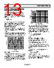
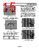
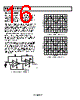
15 / 20 page  AD8510/AD8512/AD8513 Rev. E | Page 15 of 20 TIME (1 µs/DIV) VSY = ±15V CL = 500pF RL =10kΩ Figure 46. Capacitive Load Drive without Snubber When the snubber circuit is used, the overshoot is reduced from 55% to less than 3% with the same load capacitance. Ringing is virtually eliminated, as shown in Figure 47. TIME (1 µs/DIV) VSY = ±15V RL =10kΩ CL = 500pF RS =100Ω CS =1nF Figure 47. Capacitive Load with Snubber Network Optimum values for RS and CS depend on the load capacitance and input stray capacitance and are determined empirically. Table 5 shows a few values that can be used as starting points. Table 5. Optimum Values for Capacitive Loads CLOAD RS (Ω) CS 500 pF 100 1 nF 2 nF 70 100 pF 5 nF 60 300 pF OPEN-LOOP GAIN AND PHASE RESPONSE In addition to their impressive low noise, low offset voltage, and offset current, the AD8510/AD8512/AD8513 have excellent loop gain and phase response even when driving large resistive and capacitive loads. They were compared to the OPA2132 under the same conditions. With a 2.5 kΩ load at the output, the AD8510/AD8512/AD8513 have more than 8 MHz of band- width and a phase margin of more than 52°. The OPA2132, on the other hand, has only 4.5 MHz of band- width and 28° of phase margin under the same test conditions. Even with a 1 nF capacitive load in parallel with the 2 kΩ load at the output, the AD8510/AD8512/AD8513 show much better response than the OPA2132, whose phase margin is degraded to less than 0, indicating oscillation. FREQUENCY (Hz) 10k –30 –20 –10 100k 0 10 30 1M 10M 50M 40 50 20 60 70 –135 –90 –45 0 45 90 135 190 225 270 315 VSY = ±15V RL = 2.5kΩ CL = 0 Figure 48. Frequency Response of the AD8510/AD8512/AD8513 FREQUENCY (Hz) 10k –30 –20 –10 100k 0 10 30 1M 10M 50M 40 50 20 60 70 –135 –90 –45 0 45 90 135 190 225 270 315 VSY = ±15V RL = 2.5kΩ CL = 0 Figure 49. Frequency Response of the OPA2132 |
|
|
链接网址 |
| ALLDATASHEET是否为您带来帮助? [ DONATE ] |
关于 Alldatasheet | 广告服务 | 联系我们 | 隐私政策 | 数据表链接 | 链接交换 | 制造商名单 All Rights Reserved©Alldatasheet.com |
| Russian : Alldatasheetru.com | Korean : Alldatasheet.co.kr | Spanish : Alldatasheet.es | French : Alldatasheet.fr | Italian : Alldatasheetit.com Portuguese : Alldatasheetpt.com | Polish : Alldatasheet.pl | Vietnamese : Alldatasheet.vn Indian : Alldatasheet.in | Mexican : Alldatasheet.com.mx | British : Alldatasheet.co.uk | New Zealand : Alldatasheet.co.nz |
|
Family Site : ic2ic.com |
icmetro.com |
 Chinese ▼
 English
 Chinese
 German
 Japanese
 Russian
 Korean
 Spanish
 French
 Italian
 Portuguese
 Polish
 Vietnamese
 Indian
 Mexican
 British
 New Zealand