|
数据搜索系统,热门电子元器件搜索 |
|
|
数据搜索系统,热门电子元器件搜索 |
|
AD8510ARM-R2 数据表(PDF) 16 Page - Analog Devices |
|
|
|||||||||||||||||||||||||||||
AD8510ARM-R2 数据表(HTML) 16 Page - Analog Devices |
|
|
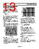
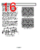
16 / 20 page  AD8510/AD8512/AD8513 Rev. E | Page 16 of 20 PRECISION RECTIFIERS TIME (1ms/DIV) Rectifying circuits are used in a multitude of applications. One of the most popular uses is in the design of regulated power supplies, where a rectifier circuit is used to convert an input sinusoid to a unipolar output voltage. There are some potential problems for amplifiers used in this manner. When the input voltage (VIN) is negative, the output is zero. The magnitude of VIN is doubled at the inputs of the op amp. This voltage can exceed the power supply voltage, which would dam- age some amplifiers permanently. The op amp must come out of saturation when VIN is negative. This delays the output signal because the amplifier requires time to enter its linear region. The AD8510/AD8512/AD8513 have a very fast overdrive recovery time, which makes them great choices for the rectification of transient signals. The symmetry of the positive and negative recovery times is also important in keeping the output signal undistorted. Figure 51. Half-Wave Rectifier Signal (Out A) TIME (1ms/DIV) Figure 50 shows the test circuit of the rectifier. The first stage of the circuit is a half-wave rectifier. When the sine wave applied at the input is positive, the output follows the input response. During the negative cycle of the input, the output tries to swing negative to follow the input, but the power supply restrains it to zero. In a similar fashion, the second stage is a follower during the positive cycle of the sine wave and an inverter during the negative cycle. 8 4 2 1 3 1/2 AD8512 4 8 5 7 6 2/2 AD8512 R2 10k Ω R3 10k Ω R1 1k Ω OUT A (HALF WAVE) OUT B (HALF WAVE) 5V 5V VIN 3V p-p Figure 52. Full-Wave Rectifier Signal (Out B) Figure 50. Half-Wave and Full-Wave Rectifier |
|
|
链接网址 |
| ALLDATASHEET是否为您带来帮助? [ DONATE ] |
关于 Alldatasheet | 广告服务 | 联系我们 | 隐私政策 | 数据表链接 | 链接交换 | 制造商名单 All Rights Reserved©Alldatasheet.com |
| Russian : Alldatasheetru.com | Korean : Alldatasheet.co.kr | Spanish : Alldatasheet.es | French : Alldatasheet.fr | Italian : Alldatasheetit.com Portuguese : Alldatasheetpt.com | Polish : Alldatasheet.pl | Vietnamese : Alldatasheet.vn Indian : Alldatasheet.in | Mexican : Alldatasheet.com.mx | British : Alldatasheet.co.uk | New Zealand : Alldatasheet.co.nz |
|
Family Site : ic2ic.com |
icmetro.com |
 Chinese ▼
 English
 Chinese
 German
 Japanese
 Russian
 Korean
 Spanish
 French
 Italian
 Portuguese
 Polish
 Vietnamese
 Indian
 Mexican
 British
 New Zealand