|
数据搜索系统,热门电子元器件搜索 |
|
|
数据搜索系统,热门电子元器件搜索 |
|
LED7708 数据表(PDF) 9 Page - STMicroelectronics |
|
|
|||||||||||||||||||||||||||||
LED7708 数据表(HTML) 9 Page - STMicroelectronics |
|
|
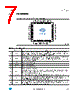
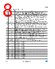
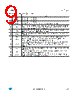
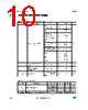
9 / 53 page  LED7708 Pin function Doc ID 022698 Rev 1 9/53 36 CH14 Driver output (channel) #14. 37 CH15 Driver output (channel) #15. 38 CH16 Driver output (channel) #16. 39 AGND Analog ground. Common return for the current generators (channels). 40 VMIN Minimum output voltage setting. Multi-level input (high, low, floating or resistor to SGND). Used in conjunction with the VFB pin to set the best output voltage range swing for a given LED array. See related section for further details. 41 CSNS External MOSFET current sense input. Connect to the sensing resistor in series with the power switch (source of the power MOSFET node). 42 PGND Power ground. Reference for the external MOSFET current sensing circuit and return for the gate driver. 43 GATE External MOSFET gate driver output. Connected to the gate of the power MOSFET. 44 VDR Gate driver supply. Internally connected to the 5 V LDO regulator. Bypass with a 1 µF ceramic capacitor to PGND as close as possible to the chip. 45 LREN 3.3 V linear regulator enable. When high or floating, the internal 3.3 V linear regulator is used to supply the device. Also used to turn off the device for power consumption reduction. To be left floating the internal 3.3 V LDO is overdriven by an external 3.3 V supply rail. 46 VIN Input of the LDO linear regulators. Bypass with a 1µF ceramic capacitor to ground as close as possible to the chip. 47 LDO3 3.3 V device supply and internal 3.3 V linear regulator output. Bypass with a 1 µF ceramic capacitor to ground as close as possible to the chip. 48 VFB Output voltage feedback for the boost controller. Connect to the central tap of the output resistor divider. See the related section for details. Table 2. Pin description (continued) Pin Function |
|
链接网址 |
| ALLDATASHEET是否为您带来帮助? [ DONATE ] |
关于 Alldatasheet | 广告服务 | 联系我们 | 隐私政策 | 数据表链接 | 链接交换 | 制造商名单 All Rights Reserved©Alldatasheet.com |
| Russian : Alldatasheetru.com | Korean : Alldatasheet.co.kr | Spanish : Alldatasheet.es | French : Alldatasheet.fr | Italian : Alldatasheetit.com Portuguese : Alldatasheetpt.com | Polish : Alldatasheet.pl | Vietnamese : Alldatasheet.vn Indian : Alldatasheet.in | Mexican : Alldatasheet.com.mx | British : Alldatasheet.co.uk | New Zealand : Alldatasheet.co.nz |
|
Family Site : ic2ic.com |
icmetro.com |
 Chinese ▼
 English
 Chinese
 German
 Japanese
 Russian
 Korean
 Spanish
 French
 Italian
 Portuguese
 Polish
 Vietnamese
 Indian
 Mexican
 British
 New Zealand