|
数据搜索系统,热门电子元器件搜索 |
|
|
数据搜索系统,热门电子元器件搜索 |
|
LED7708 数据表(PDF) 23 Page - STMicroelectronics |
|
|
|||||||||||||||||||||||||||||
LED7708 数据表(HTML) 23 Page - STMicroelectronics |
|
|
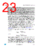
23 / 53 page  LED7708 Recommended operating conditions Doc ID 022698 Rev 1 23/53 The two signals IOK and XVOK are connected (wired-or) to all the slave devices sharing the same output voltage rail: if a channel has a low-voltage drop (below VRWL), the device that owns that channel forces low the IOK signal. In a similar way, the XVOK is released if the voltage across all the channels of a slave is higher than required (above VRWH). The wire-or connection of this signal ensures that the output voltage reduction takes place only if all the slaves (and the master itself) need this operation. Refer to the special functions section for a detailed explanation of the daisy chain connection between the master and slave devices. The boost converter is always active regardless of how many channels are active (i.e. even if all channels are off) in order to improve the load transient dynamic response. The output voltage regulation can be enabled/disabled (the OVRE bit of the DEVCFG0 register), allowing the user to perform the optimization continuously or on demand. In real applications, the spread of the forward voltage of the LEDs may cause the channels to have different voltage drops. In any case, the leading channel (i.e. the channel requiring the highest voltage to drive its LED string) is kept inside the regulation window. The reference voltage, provided by the internal DAC, spans between the minimum and maximum values, programmable through the VMIN pin (see Section 5: Electrical characteristics). As a consequence, the output voltage can be varied by the device in the following range: Equation 2 Equation 3 where R1 and R2 are the resistors of the divider connected to the output rail and VVFB is the reference voltage at the VFB pin. The LED7708 regulates the output voltage in order to optimize the overall efficiency and, to do this, it needs to read the voltage drop across the active current generators. Unfortunately, in some cases (e.g. during the soft-start phase or when all the channels are set to 0% brightness), the current generators are off and there is no useful information coming from them. Therefore the output voltage is regulated to the minimum value (Equation 2: ). It must be ensured that the minimum output voltage is below the minimum expected output voltage Table 9. Handshake signals summary Pin Function IOK Used by the slaves to increase the output voltage (algorithm is overdriven) XVOK Used by the slaves to ask for an output voltage reduction XOVF Used by the master to inform that the maximum output voltage has been reached (each slave uses this information to tag as “faulty” its open channels) XMSK Used by the master to inform the slaves that the output voltage is out of regulation and the LED fault detection must be masked to prevent false detection V BOOST min , R 1 R 2 + R 1 -------------------- ⎝⎠ ⎛⎞ V VFB min , ⋅ = V BOOST MAX , R 1 R 2 + R 1 -------------------- ⎝⎠ ⎛⎞ V VFB MAX , ⋅ = |
|
链接网址 |
| ALLDATASHEET是否为您带来帮助? [ DONATE ] |
关于 Alldatasheet | 广告服务 | 联系我们 | 隐私政策 | 数据表链接 | 链接交换 | 制造商名单 All Rights Reserved©Alldatasheet.com |
| Russian : Alldatasheetru.com | Korean : Alldatasheet.co.kr | Spanish : Alldatasheet.es | French : Alldatasheet.fr | Italian : Alldatasheetit.com Portuguese : Alldatasheetpt.com | Polish : Alldatasheet.pl | Vietnamese : Alldatasheet.vn Indian : Alldatasheet.in | Mexican : Alldatasheet.com.mx | British : Alldatasheet.co.uk | New Zealand : Alldatasheet.co.nz |
|
Family Site : ic2ic.com |
icmetro.com |
 Chinese ▼
 English
 Chinese
 German
 Japanese
 Russian
 Korean
 Spanish
 French
 Italian
 Portuguese
 Polish
 Vietnamese
 Indian
 Mexican
 British
 New Zealand