|
数据搜索系统,热门电子元器件搜索 |
|
|
数据搜索系统,热门电子元器件搜索 |
|
LED7708 数据表(PDF) 39 Page - STMicroelectronics |
|
|
|||||||||||||||||||||||||||||
LED7708 数据表(HTML) 39 Page - STMicroelectronics |
|
|
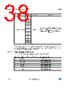
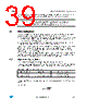
39 / 53 page  LED7708 Recommended operating conditions Doc ID 022698 Rev 1 39/53 The content of the internal registers, except the read-only bits of DEVCFG0 and DEVCFG1 (i.e. CFP, OVRS, OVFW and EDMI), is not affected when the DEN bit is cleared. Warning: In order to prevent damage to the device or to the external circuitry, some bits of DEVCFG0 and DEVCFG1 registers (CRS, SDMS and DSYS) are locked when DEN is high. 8.6 Dimming options The brightness of the LEDs connected to the output channels can be basically controlled in two ways, depending on the status of the GSME bit of the DEVCFG1 register: ● Group dimming mode (GSME=0): common dimming performed by using the brightness value received through the serial interface and stored in the BRT01 register: all the channels have the same PWM duty cycle; ● Grayscale dimming mode (GSME=1): independent PWM dimming on each channel performed by loading the BRT01:BRT16 brightness registers. In practice, a third way to control the brightness of the LEDs should rely on an intensive use of the CHSEL register by the host controller. The direct control of the CHSEL register, combined with either the group dimming or the grayscale dimming, allows the user to implement particular dimming algorithms. Once the dimming control mode has been chosen through the GSME bit, the source of the clock for the PWM generation (grayscale clock) must be selected. The LED7708 can use either an external clock source or its internal high-frequency oscillator. 8.6.1 Internal dimming oscillator The LED7708 has a programmable oscillator dedicated to the dimming circuitry. The output clock is provided at the GSCK pin for the slave devices. If the FOSC pin is forced high, the oscillator is turned off and the GSCK pin becomes the grayscale clock input. The oscillator frequency is simply set by connecting a resistor between the FOSC pin and ground: Equation 14 Table 20. FOSC pin setting options FOSC pin setting Oscillator GSCK pin function High (to LDO3) OFF Grayscale clock input Resistor to GND Active (4 MHz-25 MHz) Grayscale clock output FOSC OSC GSCK R K f = |
|
链接网址 |
| ALLDATASHEET是否为您带来帮助? [ DONATE ] |
关于 Alldatasheet | 广告服务 | 联系我们 | 隐私政策 | 数据表链接 | 链接交换 | 制造商名单 All Rights Reserved©Alldatasheet.com |
| Russian : Alldatasheetru.com | Korean : Alldatasheet.co.kr | Spanish : Alldatasheet.es | French : Alldatasheet.fr | Italian : Alldatasheetit.com Portuguese : Alldatasheetpt.com | Polish : Alldatasheet.pl | Vietnamese : Alldatasheet.vn Indian : Alldatasheet.in | Mexican : Alldatasheet.com.mx | British : Alldatasheet.co.uk | New Zealand : Alldatasheet.co.nz |
|
Family Site : ic2ic.com |
icmetro.com |
 Chinese ▼
 English
 Chinese
 German
 Japanese
 Russian
 Korean
 Spanish
 French
 Italian
 Portuguese
 Polish
 Vietnamese
 Indian
 Mexican
 British
 New Zealand