|
数据搜索系统,热门电子元器件搜索 |
|
|
数据搜索系统,热门电子元器件搜索 |
|
eZ80F91 数据表(PDF) 14 Page - Zilog, Inc. |
|
|
|||||||||||||||||||||||||||||
eZ80F91 数据表(HTML) 14 Page - Zilog, Inc. |
|
|
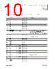
14 / 30 page  PS026102-1207 Pin Description Zdots® SBC for eZ80AcclaimPlus!™ Connectivity ASSP Product Specification 10 38 TDI/ZDA Input JTAG Data Input pin. 39 GND VSS/Ground (0 V). 40 TRIGOUT Output Active High trigger event indicator. 41 TCK/ZCL PU 10 k Ω Input JTAG Input. High on reset enables ZDI mode; Low on reset enables OCI debug. 42 TMS PU 10 k Ω Input JTAG Test Mode Select Input. 43 RTC_VDD RTC supply. For proper operation of the Zdots, this pin must be connected to the same power source that powers the module (as it is done on the Zilog® development platform). 44 EZ80CLK Output Synchronous CPU clock output. 45 I2CSCL PU 4 k Ω Bidirectional I2C Bus Clock. 46 GND VSS/Ground (0 V). 47 I2CSDA PU 4 k Ω Bidirectional I2C Data Clock. 48 GND Power VSS/Ground (0 V). 49 FlashWE PU 10 k Ω Input A Low enables a Write to external Flash memory boot block area. If this pin is unconnected, the Flash memory boot block area is Write-protected. 50 GND VSS/Ground (0 V). 51 CS3 Output Used on the eZ80190, eZ80L92, eZ80F92, eZ80F93 devices and connected to the CS8900 EMAC. 52 DIS_IRDA PU 10 k Ω Input A Low disables the onboard IRDA transceiver to use PC0/PC1 UART pins externally. 53 RESET PU 2 k Ω Bidirectional Reset Output from module or push-button reset. 54 WAIT PU 2 k Ω Input Driving the WAIT pin Low forces the CPU to provide additional clock cycles for an external peripheral or external memory to complete its Read or Write operation. 55 VCC 3.3 V supply input pin. 56 GND VSS/Ground (0 V). Table 2. Zdots Input/Output Connector Pin Identification* (Continued) Pin No Symbol Pull Up/Down Signal Direction Comments |
|
|
链接网址 |
| ALLDATASHEET是否为您带来帮助? [ DONATE ] |
关于 Alldatasheet | 广告服务 | 联系我们 | 隐私政策 | 数据表链接 | 链接交换 | 制造商名单 All Rights Reserved©Alldatasheet.com |
| Russian : Alldatasheetru.com | Korean : Alldatasheet.co.kr | Spanish : Alldatasheet.es | French : Alldatasheet.fr | Italian : Alldatasheetit.com Portuguese : Alldatasheetpt.com | Polish : Alldatasheet.pl | Vietnamese : Alldatasheet.vn Indian : Alldatasheet.in | Mexican : Alldatasheet.com.mx | British : Alldatasheet.co.uk | New Zealand : Alldatasheet.co.nz |
|
Family Site : ic2ic.com |
icmetro.com |
 Chinese ▼
 English
 Chinese
 German
 Japanese
 Russian
 Korean
 Spanish
 French
 Italian
 Portuguese
 Polish
 Vietnamese
 Indian
 Mexican
 British
 New Zealand