|
数据搜索系统,热门电子元器件搜索 |
|
|
数据搜索系统,热门电子元器件搜索 |
|
M95M01-R 数据表(PDF) 36 Page - STMicroelectronics |
|
|
|||||||||||||||||||||||||||||
M95M01-R 数据表(HTML) 36 Page - STMicroelectronics |
|
|
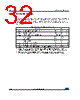
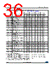
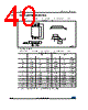
36 / 51 page  DC and AC parameters M95M01-DF M95M01-R 36/51 DocID13264 Rev 14 Table 15. AC characteristics Test conditions specified in Table 8, Table 9 and Table 10 Symbol Alt. Parameter VCC ≥ 1.7 V(1) VCC ≥ 1.8 V(2) VCC ≥ 2.5 V(3) VCC ≥ 4.5 V(1) Unit Min. Max. Min. Max. Min. Max. Min. Max. fC fSCK Clock frequency DC 2 DC 5 DC 10 DC 16 MHz tSLCH tCSS1 S active setup time 150 - 60 - 30 - 20 - ns tSHCH tCSS2 S not active setup time 150 - 60 - 30 - 20 - ns tSHSL tCS S Deselect time 200 - 60 - 40 - 25 - ns tCHSH tCSH S active hold time 150 - 60 - 30 - 20 - ns tCHSL -S not active hold time 150 - 60 - 30 - 20 - ns tCH(4) tCLH Clock high time 200 - 90 - 40 - 25 - ns tCL(4) tCLL Clock low time 200 - 90 - 40 - 25 - ns tCLCH(5) tRC Clock rise time - 2 - 2 - - - 2 µs tCHCL(5) tFC Clock fall time - 2 - 2 - - - 2 µs tDVCH tDSU Data in setup time 50 - 20 - 10 - 10 - ns tCHDX tDH Data in hold time 50 - 20 - 10 - 10 - ns tHHCH - Clock low hold time after HOLD not active 150 - 60 - 30 - 25 - ns tHLCH - Clock low hold time after HOLD active 150 - 60 - 30 - 20 - ns tCLHL - Clock low set-up time before HOLD active 0-0 - 0-0- ns tCLHH - Clock low set-up time before HOLD not active 0-0 - 0-0- ns tSHQZ(5) tDIS Output disable time - 200 - 80 - 40 - 25 ns tCLQV tV Clock low to output valid - 200 - 80 - 40 - 25 ns tCLQX tHO Output hold time 0 - 0 - 0 - 0 - ns tQLQH(5) tRO Output rise time - 200 - 80 - 40 - 25 ns tQHQL(5) tFO Output fall time - 200 - 80 - 40 - 25 ns tHHQV tLZ HOLD high to output valid - 200 - 80 - 40 - 25 ns tHLQZ(5) tHZ HOLD low to output high-Z - 200 - 80 - 40 - 25 ns tW tWC Write time -5-5-5- 5 ms 1. For devices identified by process letter K. 2. Previous products (identified with process letter A) were specified with fC(max) = 2 MHz, with the same AC values as defined in the 1.7 V columns in this table. 3. Previous products (identified with process letter A) were specified with fC(max) = 5 MHz, with the same AC values as defined in the 1.8 V columns in this table. 4. tCH + tCL must never be less than the shortest possible clock period, 1 / fC(max) 5. Value guaranteed by characterization, not 100% tested in production. |
|
链接网址 |
| ALLDATASHEET是否为您带来帮助? [ DONATE ] |
关于 Alldatasheet | 广告服务 | 联系我们 | 隐私政策 | 数据表链接 | 链接交换 | 制造商名单 All Rights Reserved©Alldatasheet.com |
| Russian : Alldatasheetru.com | Korean : Alldatasheet.co.kr | Spanish : Alldatasheet.es | French : Alldatasheet.fr | Italian : Alldatasheetit.com Portuguese : Alldatasheetpt.com | Polish : Alldatasheet.pl | Vietnamese : Alldatasheet.vn Indian : Alldatasheet.in | Mexican : Alldatasheet.com.mx | British : Alldatasheet.co.uk | New Zealand : Alldatasheet.co.nz |
|
Family Site : ic2ic.com |
icmetro.com |
 Chinese ▼
 English
 Chinese
 German
 Japanese
 Russian
 Korean
 Spanish
 French
 Italian
 Portuguese
 Polish
 Vietnamese
 Indian
 Mexican
 British
 New Zealand