|
数据搜索系统,热门电子元器件搜索 |
|
|
数据搜索系统,热门电子元器件搜索 |
|
PIP3102-R 数据表(PDF) 4 Page - NXP Semiconductors |
|
|
|||||||||||||||||||||||||||||
PIP3102-R 数据表(HTML) 4 Page - NXP Semiconductors |
|
|
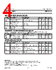
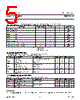
4 / 13 page  Philips Semiconductors Product Specification Logic level TOPFET PIP3102-R PROTECTION SUPPLY CHARACTERISTICS Limits are for -40˚C ≤ T mb ≤ 150˚C; typicals are for Tmb = 25˚C. SYMBOL PARAMETER CONDITIONS MIN. TYP. MAX. UNIT Protection & detection V PSF Threshold voltage 1 I F = 100 µA; VDS = 5 V 2.5 3.45 4 V Normal operation or protection latched I PS, IPSL Supply current V PS = 4.5 V - 210 450 µA V (CL)PS Clamping voltage I P = 1.5 mA 5.5 6.5 8.5 V Overload protection latched V PSR Reset voltage 1 1.8 3 V t pr Reset time V PS ≤ 1 V 10 45 120 µs OPEN CIRCUIT LOAD DETECTION CHARACTERISTICS An open circuit load condition can be detected while the TOPFET is in the off-state. Refer to TRUTH TABLE. V PS = 5 V. Limits are for -40˚C ≤ T mb ≤ 150˚C and typicals are for Tmb = 25˚C. SYMBOL PARAMETER CONDITIONS MIN. TYP. MAX. UNIT I DSP Off-state drain current 2 V IS = 0 V; 2 V ≤ VDS ≤ 40 V 0.9 1.8 2.7 mA V DSF Drain threshold voltage 3 V IS = 0 V 0.2 1 2 V V ISF Input threshold voltage 4 I D = 100 µA 0.3 0.8 1.1 V OVERLOAD CHARACTERISTICS T mb = 25˚C unless otherwise specified. SYMBOL PARAMETER CONDITIONS MIN. TYP. MAX. UNIT Short circuit load V PS > 4 V I D Drain current limiting V IS = 5 V; -40˚C ≤ T mb ≤ 150˚C 28.5 44 60 A Overload protection V PS > 4 V P D(TO) Overload power threshold device trips if P D > PD(TO) 75 185 250 W T DSC Characteristic time which determines trip time 5 250 380 600 µs Overtemperature protection V PS = 5 V T j(TO) Threshold temperature from I D ≥ 4 A or VDS > 0.2 V 150 170 - ˚C 1 When V PS is less than VPSF the flag pin indicates low protection supply voltage. Refer to TRUTH TABLE. 2 The drain source current which flows in a normal load when the protection supply is high and the input is low. 3 If V DS < VDSF then the flag indicates open circuit load. 4 For open circuit load detection, V IS must be less than VISF. 5 Trip time t d sc varies with overload dissipation PD according to the formula td sc ≈ TDSC / ln[ PD / PD(TO)]. October 2002 4 Rev 1.000 |
|
|
链接网址 |
| ALLDATASHEET是否为您带来帮助? [ DONATE ] |
关于 Alldatasheet | 广告服务 | 联系我们 | 隐私政策 | 数据表链接 | 链接交换 | 制造商名单 All Rights Reserved©Alldatasheet.com |
| Russian : Alldatasheetru.com | Korean : Alldatasheet.co.kr | Spanish : Alldatasheet.es | French : Alldatasheet.fr | Italian : Alldatasheetit.com Portuguese : Alldatasheetpt.com | Polish : Alldatasheet.pl | Vietnamese : Alldatasheet.vn Indian : Alldatasheet.in | Mexican : Alldatasheet.com.mx | British : Alldatasheet.co.uk | New Zealand : Alldatasheet.co.nz |
|
Family Site : ic2ic.com |
icmetro.com |
 Chinese ▼
 English
 Chinese
 German
 Japanese
 Russian
 Korean
 Spanish
 French
 Italian
 Portuguese
 Polish
 Vietnamese
 Indian
 Mexican
 British
 New Zealand