|
数据搜索系统,热门电子元器件搜索 |
|
|
数据搜索系统,热门电子元器件搜索 |
|
M95128-R 数据表(PDF) 20 Page - STMicroelectronics |
|
|
|||||||||||||||||||||||||||||
M95128-R 数据表(HTML) 20 Page - STMicroelectronics |
|
|
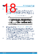
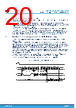
20 / 48 page  6.6.1 Cycling with error correction code (ECC x4) M95128 devices offer an error correction code (ECC) logic. The ECC is an internal logic function transparent for the SPI communication protocol. The ECC logic is implemented on each group of four EEPROM bytes (A group of four bytes is located at addresses [4*N, 4*N+1, 4*N+2, 4*N+3], where N is an integer.). Inside a group, if a single bit out of the four bytes happens to be erroneous during a Read operation, the ECC detects this bit and replaces it with the correct value. The read reliability is therefore much improved. Even if the ECC function is performed on groups of four bytes, a single byte can be written/cycled independently. In this case, the ECC function also writes/cycles the three other bytes located in the same group. As a consequence, the maximum cycling budget is defined at group level and the cycling can be distributed over the four bytes of the group: the sum of the cycles seen by byte0, byte1, byte2 and byte3 of the same group must remain below the maximum value defined in Table 13. Cycling performance by groups of four bytes. 6.7 Read Identification page (available only in M95128-D devices) The Identification page (64 bytes) is an additional page that can be written and (later) permanently locked in Read-only mode. This page is read with the Read Identification page instruction (see Table 4. Instruction set ). The Chip select signal (S) is first driven low, the bits of the instruction byte and address bytes are then shifted in, on Serial data input (D). Address bit A10 must be 0, upper address bits are Don't care, and the data byte pointed to by the lower address bits [A5:A0] is shifted out on Serial data output (Q). If Chip select (S) continues to be low, the internal address register is automatically incremented, and the byte of data at the new address is shifted out. The number of bytes to read in the ID page must not exceed the page boundary, otherwise unexpected data are read (e.g. when reading the ID page from location 24d, the number of bytes must be lower than or equal to 40d, as the ID page boundary is 64 bytes). The read cycle is terminated by driving Chip select (S) high. The rising edge of the Chip select (S) signal can occur at any time during the cycle. The first byte addressed can be any byte within any page. The instruction is not accepted, and is not executed, if a write cycle is currently in progress. Figure 15. Read Identification page sequence C D Q 15 2 1 3 4 5 6 7 8 9 10 20 21 22 23 24 25 26 27 14 13 3 2 1 0 28 29 30 7 6 5 4 3 1 7 0 High impedance Data Out 1 Instruction 16-bit address 0 MSB MSB 2 31 Data Out 2 S M95128-W M95128-R M95128-DF Read Identification page (available only in M95128-D devices) DS1356 - Rev 20 page 20/48 |
|
链接网址 |
| ALLDATASHEET是否为您带来帮助? [ DONATE ] |
关于 Alldatasheet | 广告服务 | 联系我们 | 隐私政策 | 数据表链接 | 链接交换 | 制造商名单 All Rights Reserved©Alldatasheet.com |
| Russian : Alldatasheetru.com | Korean : Alldatasheet.co.kr | Spanish : Alldatasheet.es | French : Alldatasheet.fr | Italian : Alldatasheetit.com Portuguese : Alldatasheetpt.com | Polish : Alldatasheet.pl | Vietnamese : Alldatasheet.vn Indian : Alldatasheet.in | Mexican : Alldatasheet.com.mx | British : Alldatasheet.co.uk | New Zealand : Alldatasheet.co.nz |
|
Family Site : ic2ic.com |
icmetro.com |
 Chinese ▼
 English
 Chinese
 German
 Japanese
 Russian
 Korean
 Spanish
 French
 Italian
 Portuguese
 Polish
 Vietnamese
 Indian
 Mexican
 British
 New Zealand