|
数据搜索系统,热门电子元器件搜索 |
|
|
数据搜索系统,热门电子元器件搜索 |
|
STV-6101-R01 数据表(PDF) 8 Page - STMicroelectronics |
|
|
|||||||||||||||||||||||||||||
STV-6101-R01 数据表(HTML) 8 Page - STMicroelectronics |
|
|
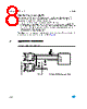
8 / 17 page  Application information VM6101 8/17 2.4.2 Alternate slave address selection After power-on or after resuming from power-down, the 7-bit slave address is 0x10. If another slave device shares the same address, it is possible to remap the VM6101 to address 0x11 by performing the following operations: 1. Connect the INT pin to a pull-up resistor to VDD (1 MΩ typ.). 2. After power-on or power-down resume, issue a write command to set the ADDR_SEL bit of CONTROL register (i.e. write 0x10 at register address 0x02, slave address 0x10). 3. At this time, the VM6101 samples the INT pin and sets its slave address accordingly: INT sampled low: 7-bit address = 0x10, INT sampled high: 7-bit address = 0x11. Two VM6101 can thus coexist on the same bus; one should have its INT pin pulled low, the other one should have its INT pin pulled high (see Figure 5.). 3 Application information Figure 5. Application diagram Host Microcontroller VM6101 SCL SDA INT VDD GND PD +3.3V SCL SDA GPIO0 GPIO1 +3.3V GPIO2 GPIO3 TEST AMUX NC VM6101 SCL SDA INT VDD GND PD +3.3V TEST AMUX NC +3.3V I²C 7-bit addr = 0x10 I²C 7-bit addr = 0x11 Optional Note: Rb value depends on bus capacitive load |
|
|
链接网址 |
| ALLDATASHEET是否为您带来帮助? [ DONATE ] |
关于 Alldatasheet | 广告服务 | 联系我们 | 隐私政策 | 数据表链接 | 链接交换 | 制造商名单 All Rights Reserved©Alldatasheet.com |
| Russian : Alldatasheetru.com | Korean : Alldatasheet.co.kr | Spanish : Alldatasheet.es | French : Alldatasheet.fr | Italian : Alldatasheetit.com Portuguese : Alldatasheetpt.com | Polish : Alldatasheet.pl | Vietnamese : Alldatasheet.vn Indian : Alldatasheet.in | Mexican : Alldatasheet.com.mx | British : Alldatasheet.co.uk | New Zealand : Alldatasheet.co.nz |
|
Family Site : ic2ic.com |
icmetro.com |
 Chinese ▼
 English
 Chinese
 German
 Japanese
 Russian
 Korean
 Spanish
 French
 Italian
 Portuguese
 Polish
 Vietnamese
 Indian
 Mexican
 British
 New Zealand