|
数据搜索系统,热门电子元器件搜索 |
|
|
数据搜索系统,热门电子元器件搜索 |
|
STV-6101-R01 数据表(PDF) 9 Page - STMicroelectronics |
|
|
|||||||||||||||||||||||||||||
STV-6101-R01 数据表(HTML) 9 Page - STMicroelectronics |
|
|
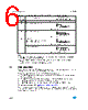
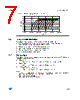
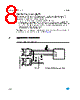
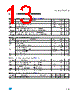
9 / 17 page  VM6101 Register description 9/17 4 Register description Note: RO = Read Only; RW = Read/Write. Reserved bits must be written with 0s and return 0 upon read; Reserved bytes must not be accessed otherwise unpredictable results my occur. Table 3. Register description Addr. Bits Def. Name Description 0x00 [3:0] 1 REVISION Chip revision (RO). 0x00 [7:4] 0 MASK Mask code (RO). 0x01 [7:0] 0x04 N_PIXEL (RO) 0x02 [6:0] 0x04 CONTROL Control register (RW) [1:0] 0 CHSEL Channel select for comparator and PWM logic: 0: Y 1: R 2: G 3: B 2 1 INT_FSEL INT pin function select: 0: PWM generator output 1: Comparator logic output 3 0 PWM_POL PWM polarity: 0: Normal (Thin pulse for low values, Wide pulses for high values) 1: Inverted. 4 0 ADDR_SEL Address Select: when written with ‘1’, the INT pin goes high impedance; after a duration T (defined below), the INT pin is sampled and returns to low impedance. The device slave address is set accordingly: INT sampled low: address = 0x20 INT sampled high: address = 0x22. [6:5] 0 ADDR_SELW Address select sampling window duration: 0: T = 160 µs (default) 1: T = 80 µs 2: T = 40 µs 3: T = 20 us This duration allows for INT pin pull-up rise time. 70 Reserved 0x03 [7:0] 0 Reserved (RO). 0x04 [2:0] 0x01 Y_STATUS Y-channel status register (RO). Reading this register will cause Y_CNT to be transferred to serial interface buffer. 5 MSBs are read as zeros. 0 1 RESET This bit is set after reset. Cleared after first read of STATUS register. 1 0 OVERFLOW This bit is set upon counter overflow: current counter values are invalid. 2 0 READY When set, indicates that a new count value is available in the 4 registers here below. |
|
|
链接网址 |
| ALLDATASHEET是否为您带来帮助? [ DONATE ] |
关于 Alldatasheet | 广告服务 | 联系我们 | 隐私政策 | 数据表链接 | 链接交换 | 制造商名单 All Rights Reserved©Alldatasheet.com |
| Russian : Alldatasheetru.com | Korean : Alldatasheet.co.kr | Spanish : Alldatasheet.es | French : Alldatasheet.fr | Italian : Alldatasheetit.com Portuguese : Alldatasheetpt.com | Polish : Alldatasheet.pl | Vietnamese : Alldatasheet.vn Indian : Alldatasheet.in | Mexican : Alldatasheet.com.mx | British : Alldatasheet.co.uk | New Zealand : Alldatasheet.co.nz |
|
Family Site : ic2ic.com |
icmetro.com |
 Chinese ▼
 English
 Chinese
 German
 Japanese
 Russian
 Korean
 Spanish
 French
 Italian
 Portuguese
 Polish
 Vietnamese
 Indian
 Mexican
 British
 New Zealand