|
数据搜索系统,热门电子元器件搜索 |
|
|
数据搜索系统,热门电子元器件搜索 |
|
STDRIVE102HTR 数据表(PDF) 16 Page - STMicroelectronics |
|
|
|||||||||||||||||||||||||||||
STDRIVE102HTR 数据表(HTML) 16 Page - STMicroelectronics |
|
|
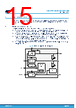
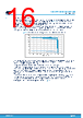
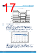
16 / 56 page  5.1.1 12 V LDO linear regulator This regulator generates the voltage on the VCC pin, which is the supply of the low-side gate drivers and the set point for the 'VBOOT - VM' voltage provided by the charge pump (refer to Section 5.1.3). A low ESR ceramic capacitor of 4.7 µF, 25 V must be placed as close as possible to the VCC pin, to ensure the stability of the VCC and support the currents required by the low-side gate drivers. In addition, external loads can be connected to VCC pin, taking care to stay within the operating range. The output current of the regulator is limited at ICC,lim protecting it against short circuit and overload. The overall consumption of the external loads plus the drivers must be smaller than this current limitation. Figure 6. 12 V LDO output according to the current load at different VS input 5 6 7 8 9 10 11 12 13 0 10 20 30 40 50 60 70 80 90 Load current [mA] VS > 13 V VS = 12 V VS = 6 V The linear regulator input is connected to the main supply VS. The regulator can be bypassed by connecting the VCC and the VS together and forcing an external voltage equal to the target VCC value, which must be in any case within the operative range of the VCC pin. The regulator is disabled in standby mode in order to reduce the current consumption. In case the VCC voltage falls below the UVLO threshold (VCC(Off)), the gate drivers turn off all the external MOSFETs, forcing the power stage into a safe condition. Concurrently, the nFAULT open-drain pin is forced low to signal that the UVLO protection has been triggered. As soon as the VCC voltage rises above the VCC(On) threshold, the nFAULT is released and the drivers return to an active condition, according to the status of the digital inputs. In the STDRIVE102BH only when the VCC voltage falls below the “power-good” threshold (VP_GOOD(Off)), the FLAG open-drain pin is forced low, but there are no other effects on the functional blocks of the devices. The FLAG pin is then released as soon as the VCC voltage rises above the VP_GOOD(On) threshold. An example of the VCC thresholds management is shown in Figure 7. STDRIVE102BH, STDRIVE102H Device description DS14545 - Rev 1 page 16/56 |
|
链接网址 |
| ALLDATASHEET是否为您带来帮助? [ DONATE ] |
关于 Alldatasheet | 广告服务 | 联系我们 | 隐私政策 | 数据表链接 | 链接交换 | 制造商名单 All Rights Reserved©Alldatasheet.com |
| Russian : Alldatasheetru.com | Korean : Alldatasheet.co.kr | Spanish : Alldatasheet.es | French : Alldatasheet.fr | Italian : Alldatasheetit.com Portuguese : Alldatasheetpt.com | Polish : Alldatasheet.pl | Vietnamese : Alldatasheet.vn Indian : Alldatasheet.in | Mexican : Alldatasheet.com.mx | British : Alldatasheet.co.uk | New Zealand : Alldatasheet.co.nz |
|
Family Site : ic2ic.com |
icmetro.com |
 Chinese ▼
 English
 Chinese
 German
 Japanese
 Russian
 Korean
 Spanish
 French
 Italian
 Portuguese
 Polish
 Vietnamese
 Indian
 Mexican
 British
 New Zealand