|
数据搜索系统,热门电子元器件搜索 |
|
|
数据搜索系统,热门电子元器件搜索 |
|
FT201XS-R 数据表(PDF) 39 Page - Future Technology Devices International Ltd. |
|
|
|||||||||||||||||||||||||||||
FT201XS-R 数据表(HTML) 39 Page - Future Technology Devices International Ltd. |
|
|
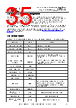
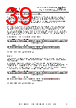
39 / 49 page  Copyright © 2014 Future Technology Devices International Limited 39 FT201X USB I2C SLAVE IC Datasheet Version 1.4 Document No.: FT_000627 Clearance No.: FTDI# 264 10.5.4 Examples of Writing and Reading When performing MTP memory write and read requests via the I2C protocol, users must first issue the MTP address command along with 2 bytes representing the MTP memory address. The acknowledge phase of this command represents the current status of the MTP memory (whether it is busy or not). If the MTP memory is being accessed during an I2C access then the respective command and data phases will NAK the master. The address will only be updated when the MTP memory is inactive. Writing The first part of the communication sets the address, and this is followed by the write command along with the data to be written. The MTP memory write itself will be initiated when the FT201X receives an MTP memory write command followed by a single data byte. The ACK phase represents the current activity of the MTP memory (whether it is busy or not busy). A successful write will only occur when both status phases acknowledge the master indicating that the MTP memory can start the write. Users wishing to determine if the MTP memory write was successful should immediately try an MTP memory read to verify the new contents. This process of writing to the MTP memory is shown below: Figure 10.2: Write EEPROM command sequence Reading In a similar way, the read is carried out as shown below.The first part of the communication sets the address, and this is followed by the read command and a read cycle used to retrieve the data read back from that address. An MTP memory read will be initiated when the I2C slave receives an MTP read command. The acknowledge during the command phase indicates whether or not the MTP memory will be able to service the read request. If it is possible to carry out the read, the I2C moves into the data phase where it can either continue with the read transaction until the slave successful returns an ACK along with the data or if it receives NAK during the data phase it can abort the read transfer and try again. Figure 10.3: Read EEPROM command sequence 0000000 0 0001_0000 0 S/Sr General call addr R/!W A MTP ADDR cmd A/!A Sr Slave addr R/!W A MTP ADR MSB A A 0000000 0 0001_0010 0 S/Sr General call addr R/!W A MTP WR cmd A/!A Sr Slave addr R/!W A MTP WR DATA A P/Sr MTP Memory Address Phase MTP memory Write Phase MTP ADR LSB 0000000 0 0001_0000 0 S/Sr General call addr R/!W A MTP ADDR cmd A/!A Sr Slave addr R/!W A MTP ADR MSB A A 0000000 0 0001_0100 1 S/Sr General call addr R/!W A MTP WR cmd A/!A Sr Slave addr R/!W A MTP WR DATA A P/Sr MTP ADR LSB MTP Memory Address Phase MTP memory Read Phase |
|
链接网址 |
| ALLDATASHEET是否为您带来帮助? [ DONATE ] |
关于 Alldatasheet | 广告服务 | 联系我们 | 隐私政策 | 数据表链接 | 链接交换 | 制造商名单 All Rights Reserved©Alldatasheet.com |
| Russian : Alldatasheetru.com | Korean : Alldatasheet.co.kr | Spanish : Alldatasheet.es | French : Alldatasheet.fr | Italian : Alldatasheetit.com Portuguese : Alldatasheetpt.com | Polish : Alldatasheet.pl | Vietnamese : Alldatasheet.vn Indian : Alldatasheet.in | Mexican : Alldatasheet.com.mx | British : Alldatasheet.co.uk | New Zealand : Alldatasheet.co.nz |
|
Family Site : ic2ic.com |
icmetro.com |
 Chinese ▼
 English
 Chinese
 German
 Japanese
 Russian
 Korean
 Spanish
 French
 Italian
 Portuguese
 Polish
 Vietnamese
 Indian
 Mexican
 British
 New Zealand