|
数据搜索系统,热门电子元器件搜索 |
|
|
数据搜索系统,热门电子元器件搜索 |
|
RC19302A00AGNT#BD0 数据表(PDF) 29 Page - Renesas Technology Corp |
|
|
|||||||||||||||||||||||||||||
RC19302A00AGNT#BD0 数据表(HTML) 29 Page - Renesas Technology Corp |
|
|
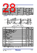
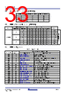
29 / 62 page  R31DS0210EU0106 Rev.1.06 Page 29 May 11, 2026 RC193xx Datasheet 2. A host should not drive the clock at a frequency below the minimum fSMB. Further, the operating clock frequency should not be reduced below the minimum value of fSMB due to periodic clock extending by target devices as defined in Section 5.3.3 of System Management Bus (SMBus) Specification, Version 3.2, dated 12 Jan, 2022. This limit does not apply to the bus idle condition, and this limit is independent from the tLOW: SEXT and tLOW: MEXT limits. For example, if the SCLK is high for tHIGH,MAX, the clock must not be periodically stretched longer than 1/fSMB,MIN – tHIGH,MAX. This requirement does not pertain to a device that extends the SCLK low for data processing of a received byte, data buffering and so forth for longer than 100 µs in a non-periodic way. 3. A device must internally provide sufficient hold time for the SDATA signal (with respect to the VIH,MIN of the SCLK signal) to bridge the undefined region of the falling edge of SCLK. 4. Target devices may have caused other target devices to hold SDA low. This is the maximum time that a device can hold SDATA low after the host raises SCLK after the last bit of a transaction. A target device may detect how long SDA is held low and release SDA after the time out period. 5. Devices participating in a transfer can abort the transfer in progress and release the bus when any single clock low interval exceeds the value of tTIMEOUT,MIN. After the host in a transaction detects this condition, it must generate a stop condition within or after the current data byte in the transfer process. Devices that have detected this condition must reset their communication and be able to receive a new START condition no later than tTIMEOUT,MAX. Typical device examples include the host controller, and embedded controller, and most devices that can host the SMBus. Some simple devices do not contain a clock low drive circuit; this simple kind of device typically may reset its communications port after a start or a stop condition. A timeout condition can only be ensured if the device that is forcing the timeout holds the SCLK low for tTIMEOUT,MAX or longer. 6. The device has the option of detecting a timeout if the SDATAA pin is also low for this time. 7. tHIGH,MAX provides a simple guaranteed method for hosts to detect bus idle conditions. A host can assume that the bus is free if it detects that the clock and data signals have been high for greater than tHIGH,MAX. 8. tLOW:MEXT is the cumulative time a host device is allowed to extend its clock cycles within each byte of a message as defined from START-to- ACK, ACK-to-ACK, or ACK-to-STOP. It is possible that a target device or another host will also extend the clock causing the combined clock low time to be greater than tLOW:MEXT on a given byte. This parameter is measured with a full speed target device as the sole target of the host. 9. The rise and fall time measurement limits are defined as follows: ▪ Rise Time Limits: (VIL:MAX - 0.15 V) to (VIH:MIN + 0.15 V) ▪ Fall Time Limits: (VIH:MIN + 0.15 V) to (VIL:MAX - 0.15 V) 10. Devices must provide a means to reject noise spikes of a duration up to the maximum specified value. |
|
链接网址 |
| ALLDATASHEET是否为您带来帮助? [ DONATE ] |
关于 Alldatasheet | 广告服务 | 联系我们 | 隐私政策 | 数据表链接 | 链接交换 | 制造商名单 All Rights Reserved©Alldatasheet.com |
| Russian : Alldatasheetru.com | Korean : Alldatasheet.co.kr | Spanish : Alldatasheet.es | French : Alldatasheet.fr | Italian : Alldatasheetit.com Portuguese : Alldatasheetpt.com | Polish : Alldatasheet.pl | Vietnamese : Alldatasheet.vn Indian : Alldatasheet.in | Mexican : Alldatasheet.com.mx | British : Alldatasheet.co.uk | New Zealand : Alldatasheet.co.nz |
|
Family Site : ic2ic.com |
icmetro.com |
 Chinese ▼
 English
 Chinese
 German
 Japanese
 Russian
 Korean
 Spanish
 French
 Italian
 Portuguese
 Polish
 Vietnamese
 Indian
 Mexican
 British
 New Zealand