|
数据搜索系统,热门电子元器件搜索 |
|
|
数据搜索系统,热门电子元器件搜索 |
|
RC19302A00AGNT#BD0 数据表(PDF) 13 Page - Renesas Technology Corp |
|
|
|||||||||||||||||||||||||||||
RC19302A00AGNT#BD0 数据表(HTML) 13 Page - Renesas Technology Corp |
|
|
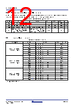
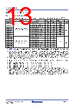
13 / 62 page  R31DS0210EU0106 Rev.1.06 Page 13 May 11, 2026 RC193xx Datasheet 2.4 Electrical Characteristics 2.4.1 Additive Phase Jitter Table 7. PCIe Refclk Phase Jitter (CLKSEL_tri = 0 or 1, Unselected CLKIN Off) – Normal Conditions [1][2][3] 1. The Refclk jitter is measured after applying the filter functions found in the PCI Express Base Specification 7.0. For the exact measurement setup, see Test Loads. The worst case results for each data rate are summarized in this table. Equipment noise is removed from all measurements. 2. Jitter measurements are made with a capture of at least 100,000 clock cycles captured by a real-time oscilloscope (RTO) with a sample rate of 20GS/s or greater. Broadband oscilloscope noise must be minimized in the measurement. The measured PP jitter is used (no extrapolation) for RTO measurements. Alternately, jitter measurements can be made with a Phase Noise Analyzer (PNA) extending (flat) and integrating and folding the frequency content up to an offset from the carrier frequency of at least 200MHz (at 300MHz absolute frequency) below the Nyquist frequency. For PNA measurements for the 2.5GT/s data rate, the RMS jitter is converted to peak-to-peak jitter using a multiplication factor of 8.83. 3. Differential input swing ≥ 1600mV and input slew rate ≥ 3.5V/ns. The rms sum of the source jitter and the additive jitter (arithmetic sum for PCIe Gen1) must be less than the jitter specification listed Symbol Parameter Condition Typical Maximum Spec. Limit Unit tjphPCIeG1-CC Additive PCIe Phase Jitter (Common Clocked Architecture) PCIe Gen1 (2.5 GT/s) 418 658 86,000 fs p-p tjphPCIeG2-CC PCIe Gen2 Hi Band (5.0 GT/s) 52 74 3,100 fs RMS PCIe Gen2 Lo Band (5.0 GT/s) 21 23 3,000 tjphPCIeG3-CC PCIe Gen3 (8.0 GT/s) 18 25 1,000 tjphPCIeG4-CC PCIe Gen4 (16.0 GT/s) [4][5] 4. SSC spurs from the fundamental and harmonics are removed up to a cutoff frequency of 2MHz taking care to minimize removal of any non-SSC content. 5. Note that 0.7ps RMS is to be used in channel simulations to account for additional noise in a real system. 18 25 500 tjphPCIeG5-CC PCIe Gen5 (32.0 GT/s) [4] [6] 6. Note that 0.25ps RMS is to be used in channel simulations to account for additional noise in a real system. 6.9 9.8 150 tjphPCIeG6-CC PCIe Gen6 (64.0 GT/s) [4] [7] 7. Note that 0.15ps RMS is to be used in channel simulations to account for additional noise in a real system. 4.1 5.8 100 tjphPCIeG7-CC PCIe Gen7 (128 GT/s) [4][8] 8. Note that 0.10ps RMS is to be used in channel simulations to account for additional noise in a real system. 2.9 4.0 67 tjphPCIeG2-IR Additive PCIe Phase Jitter (IR Architectures) PCIe Gen2 (5.0 GT/s) 47 60 [9] 9. The PCI Express Base Specification 7.0 provides the filters necessary to calculate SRIS jitter values; it does not provide specification limits, therefore, the reference to this footnote in the Limit column. SRIS values are informative only. A common practice is to split the common clock budget in half. For 16GT/s data rates and above, the user must choose whether to use the output jitter specification, or the input jitter specification, which includes an allocation for the jitter added by the channel. Using 32GT/s, the Refclk jitter budget is 150fs RMS. One half of the Refclk jitter budget is 106fs RMS. At the clock input, the system must deliver 250fs RMS. One half of this value is 177fs RMS. If the clock is placed next to the PCIe device in an SRIS system, the channel is very short and the user can choose to use this more relaxed value as the jitter limit. fs RMS tjphPCIeG3-IR PCIe Gen3 (8.0 GT/s) 18 24 tjphPCIeG4-IR PCIe Gen4 (16.0 GT/s) [3] [4] 19 25 tjphPCIeG5-IR PCIe Gen5 (32.0 GT/s) [3] [5] 5.1 6.9 tjphPCIeG6-IR PCIe Gen6 (64.0 GT/s) [3] [7] 3.7 4.9 tjphPCIeG7-IR PCIe Gen7 (128 GT/s) [3][7] 2.6 3.4 |
|
链接网址 |
| ALLDATASHEET是否为您带来帮助? [ DONATE ] |
关于 Alldatasheet | 广告服务 | 联系我们 | 隐私政策 | 数据表链接 | 链接交换 | 制造商名单 All Rights Reserved©Alldatasheet.com |
| Russian : Alldatasheetru.com | Korean : Alldatasheet.co.kr | Spanish : Alldatasheet.es | French : Alldatasheet.fr | Italian : Alldatasheetit.com Portuguese : Alldatasheetpt.com | Polish : Alldatasheet.pl | Vietnamese : Alldatasheet.vn Indian : Alldatasheet.in | Mexican : Alldatasheet.com.mx | British : Alldatasheet.co.uk | New Zealand : Alldatasheet.co.nz |
|
Family Site : ic2ic.com |
icmetro.com |
 Chinese ▼
 English
 Chinese
 German
 Japanese
 Russian
 Korean
 Spanish
 French
 Italian
 Portuguese
 Polish
 Vietnamese
 Indian
 Mexican
 British
 New Zealand