|
数据搜索系统,热门电子元器件搜索 |
|
|
数据搜索系统,热门电子元器件搜索 |
|
RC19302A00AGNT#BD0 数据表(PDF) 48 Page - Renesas Technology Corp |
|
|
|||||||||||||||||||||||||||||
RC19302A00AGNT#BD0 数据表(HTML) 48 Page - Renesas Technology Corp |
|
|
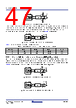
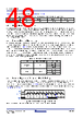
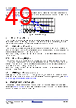
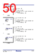
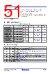
48 / 62 page  R31DS0210EU0106 Rev.1.06 Page 48 May 11, 2026 RC193xx Datasheet Table 34 contains values for the items in Figure 20 and Figure 21. 5.4 Power Down Tolerant Pins Pins labeled Power Down Tolerant (PDT) can be driven by voltages as high as the normal VDD of the chip, even though VDD is not present (the device is not powered). There will be no ill effects to the device and it will power up normally. This feature supports disaggregation, where the RC193xx may be on one circuit board and devices that interface with it are on other boards. These boards may power up at different times, driving pins on the RC193xx before it has received power. NOTE: The differential CLKIN pins are limited to 1.4V. Applying a voltage higher than this may damage the part. 5.5 Flexible Startup Sequencing RC193xx devices support Flexible Startup Sequencing (FSS). FSS allows application of CLKIN at different times in the device/system startup sequence. FSS is an additional feature that helps the system designer manage the impact of disaggregation. Table 35 shows the supported sequences; that is, the RC193xx devices can have CLKIN running before VDD is applied, and can have VDD applied and sit for extended periods with no input clock. Note: The PWRGD_PWRDNb is synchronized with the selected CLKIN. If CLKIN is not present, the RC193xx will not sample the pin until CLKIN is present. This applies to both powering up and powering down. If powered up when the input clock stops, ACP (default enabled) will place the outputs into a low/low state even though the RC193xx will not be completely powered down. 5.6 Loss of Signal and Automatic Clock Parking The RC193xx devices have a Loss of Signal (LOS) circuit to detect the presence or absence of an input clock. The LOS circuit drives the open-drain LOSb pin (the “b” suffix indicates “bar”, or active-low) and sets the LOS_EVT bit in the SMBus register space. Figure 22 shows the LOSb de-assertion timing for the RC193xx clock multiplexers. LOSb on the RC193xx multiplexers defaults to low at power up. CLKIN is represented differentially in Figure 22 and Figure 23. Figure 22. LOSb De-assert Timing RC193xx Devices Note: The LOSb pin monitors the selected input clock in the RC193xx multiplexers. Table 34. Parameters for Direct-Coupled Receiver-Terminated Configurations ZOUT_SEL_tri ZO (ohms) ZDIF (ohms) RP (ohms) RT (ohms) M 34 100 ZDIF /2 ZDIF Table 35. Flexible Startup Sequences VDD PWRGD_PWRDNb CLKIN/CLKINb Not present X Running Floating Low/Low Present 0 or 1 Running Floating Low/Low VDD CLKIN LOSb LOSDeassert typ LOSDeassert max c e d f |
|
链接网址 |
| ALLDATASHEET是否为您带来帮助? [ DONATE ] |
关于 Alldatasheet | 广告服务 | 联系我们 | 隐私政策 | 数据表链接 | 链接交换 | 制造商名单 All Rights Reserved©Alldatasheet.com |
| Russian : Alldatasheetru.com | Korean : Alldatasheet.co.kr | Spanish : Alldatasheet.es | French : Alldatasheet.fr | Italian : Alldatasheetit.com Portuguese : Alldatasheetpt.com | Polish : Alldatasheet.pl | Vietnamese : Alldatasheet.vn Indian : Alldatasheet.in | Mexican : Alldatasheet.com.mx | British : Alldatasheet.co.uk | New Zealand : Alldatasheet.co.nz |
|
Family Site : ic2ic.com |
icmetro.com |
 Chinese ▼
 English
 Chinese
 German
 Japanese
 Russian
 Korean
 Spanish
 French
 Italian
 Portuguese
 Polish
 Vietnamese
 Indian
 Mexican
 British
 New Zealand