|
数据搜索系统,热门电子元器件搜索 |
|
|
数据搜索系统,热门电子元器件搜索 |
|
TDF8591TH 数据表(PDF) 4 Page - NXP Semiconductors |
|
|
|||||||||||||||||||||||||||||
TDF8591TH 数据表(HTML) 4 Page - NXP Semiconductors |
|
|
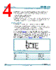
4 / 34 page  TDF8591TH_1 © NXP B.V. 2008. All rights reserved. Product data sheet Rev. 01 — 5 March 2008 4 of 34 NXP Semiconductors TDF8591TH 2 × 100 W SE (4 Ω) or 1 × 310 W BTL (4 Ω) class-D amplifier The TDF8591TH contains two independent amplifier channels with a differential input stage, high output power, high efficiency (90 %), low distortion and a low quiescent current. The amplifier channels can be connected in the following configurations: • Mono Bridge-Tied Load (BTL) amplifier • Dual Single-Ended (SE) amplifiers The TDF8591TH also contains circuits common to both channels such as the oscillator, all reference sources, the mode functionality and a digital timing manager. For protection a thermal foldback, temperature, current and voltage protection are built in. 6.2 Mode selection The TDF8591TH can be switched in three operating modes via pin MODE: • Standby mode; the amplifiers are switched off to achieve a very low supply current • Mute mode; the amplifiers are switching idle (50 % duty cycle), but the audio signal at the output is suppressed by disabling the VI-converter input stages • Operating mode; the amplifiers are fully operational with output signal The input stage (see Figure 1) contributes to the DC offset measured at the amplifier output. To avoid pop noise the DC output offset voltage should be increased gradually at a mode transition from mute to operating, or vice versa, by limiting the dVMODE/dt on pin MODE, resulting in a small dVO(offset)/dt for the DC output offset voltage. The required time constant for a gradually increase of the DC output offset voltage between mute and operating is generated via an RC network on pin MODE. An example of a switching circuit for driving pin MODE is illustrated in Figure 3 and explained in Table 3. Fig 3. Example of mode selection circuit Table 3. Mode selection S1 S2 Mode selection closed closed Standby mode closed open Standby mode open closed Mute mode open open Operating mode 001aad836 5.6 k Ω 5.6 k Ω 5.6 V 5.6 k Ω S1 S2 MODE SGND 100 µF (10 V) VDDP |
|
链接网址 |
| ALLDATASHEET是否为您带来帮助? [ DONATE ] |
关于 Alldatasheet | 广告服务 | 联系我们 | 隐私政策 | 数据表链接 | 链接交换 | 制造商名单 All Rights Reserved©Alldatasheet.com |
| Russian : Alldatasheetru.com | Korean : Alldatasheet.co.kr | Spanish : Alldatasheet.es | French : Alldatasheet.fr | Italian : Alldatasheetit.com Portuguese : Alldatasheetpt.com | Polish : Alldatasheet.pl | Vietnamese : Alldatasheet.vn Indian : Alldatasheet.in | Mexican : Alldatasheet.com.mx | British : Alldatasheet.co.uk | New Zealand : Alldatasheet.co.nz |
|
Family Site : ic2ic.com |
icmetro.com |
 Chinese ▼
 English
 Chinese
 German
 Japanese
 Russian
 Korean
 Spanish
 French
 Italian
 Portuguese
 Polish
 Vietnamese
 Indian
 Mexican
 British
 New Zealand