|
数据搜索系统,热门电子元器件搜索 |
|
|
数据搜索系统,热门电子元器件搜索 |
|
TDF8591TH 数据表(PDF) 9 Page - NXP Semiconductors |
|
|
|||||||||||||||||||||||||||||
TDF8591TH 数据表(HTML) 9 Page - NXP Semiconductors |
|
|
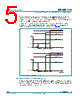
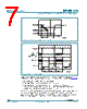
9 / 34 page  TDF8591TH_1 © NXP B.V. 2008. All rights reserved. Product data sheet Rev. 01 — 5 March 2008 9 of 34 NXP Semiconductors TDF8591TH 2 × 100 W SE (4 Ω) or 1 × 310 W BTL (4 Ω) class-D amplifier [3] Only complete shut down of amplifier in case of a short-circuit. In all other cases current limiting resulting in clipping output signal. [4] Fault condition detected during (every) transition between standby-to-mute and during restart after activation of OCP (short-circuit to one of the supply lines). 6.5 Diagnostic output Pin DIAG is pulled LOW when the OCP is triggered. With a continuous short-circuited load a switching pattern in the voltage on pin DIAG is observed (see Figure 6). A permanent LOW on pin DIAG indicates a short-circuit to the supply lines whereas a short-circuited load causes a switching DIAG pin (see Section 6.4.3). The pin DIAG reference voltage is VSSA. Pin DIAG should not be connected to an external pull-up. An example of a circuit to read out and level shift the diagnostic data is given in Figure 7. V5V represents a logic supply that is used in the application by the microprocessor that reads out the DIAG data. 6.6 Differential inputs For a high Common Mode Rejection Ratio (CMRR) and a maximum of flexibility in the application, the audio inputs are fully differential. By connecting the inputs anti-parallel the phase of one of the channels can be inverted, so that a load can be connected between the two output filters. In this case the system operates as a mono BTL amplifier. The input configuration for a mono BTL application is illustrated in Figure 8. In the stereo SE configuration it is also recommended to connect the two differential inputs in anti-phase. This has advantages for the current handling of the supply voltage at low signal frequencies (supply pumping). Fig 7. DIAG readout circuit with level shift 001aad840 100 k Ω 100 k Ω 27 k Ω 5.6 V 10 k Ω VDDA VSSA DIAG DIAG out SGND M2 V5V M1 |
|
链接网址 |
| ALLDATASHEET是否为您带来帮助? [ DONATE ] |
关于 Alldatasheet | 广告服务 | 联系我们 | 隐私政策 | 数据表链接 | 链接交换 | 制造商名单 All Rights Reserved©Alldatasheet.com |
| Russian : Alldatasheetru.com | Korean : Alldatasheet.co.kr | Spanish : Alldatasheet.es | French : Alldatasheet.fr | Italian : Alldatasheetit.com Portuguese : Alldatasheetpt.com | Polish : Alldatasheet.pl | Vietnamese : Alldatasheet.vn Indian : Alldatasheet.in | Mexican : Alldatasheet.com.mx | British : Alldatasheet.co.uk | New Zealand : Alldatasheet.co.nz |
|
Family Site : ic2ic.com |
icmetro.com |
 Chinese ▼
 English
 Chinese
 German
 Japanese
 Russian
 Korean
 Spanish
 French
 Italian
 Portuguese
 Polish
 Vietnamese
 Indian
 Mexican
 British
 New Zealand