|
数据搜索系统,热门电子元器件搜索 |
|
|
数据搜索系统,热门电子元器件搜索 |
|
TDF8591TH 数据表(PDF) 5 Page - NXP Semiconductors |
|
|
|||||||||||||||||||||||||||||
TDF8591TH 数据表(HTML) 5 Page - NXP Semiconductors |
|
|
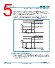
5 / 34 page  TDF8591TH_1 © NXP B.V. 2008. All rights reserved. Product data sheet Rev. 01 — 5 March 2008 5 of 34 NXP Semiconductors TDF8591TH 2 × 100 W SE (4 Ω) or 1 × 310 W BTL (4 Ω) class-D amplifier The value of the RC time constant should be dimensioned for 500 ms. If the 100 µF capacitor is left out of the application the voltage on pin MODE will be applied with a much smaller time constant, which might result in audible pop noises during start-up (depending on DC output offset voltage and used loudspeaker). In order to fully charge the coupling capacitors at the inputs, the amplifier will remain automatically in Mute mode for approximately 150 ms before switching to Operating mode. A complete overview of the start-up timing is given in Figure 4. 6.3 Pulse width modulation frequency The output signal of the amplifier is a PWM signal with a switching frequency that is set by an external resistor Rext(OSC) connected between pins OSC and VSSA. An optimum setting for the carrier frequency is between 300 kHz and 350 kHz. An external resistor Rext(OSC) of 30 k Ω sets the frequency to 310 kHz. Fig 4. Timing on mode selection input audio operating mute standby 5 V 2.5 V 0 V (SGND) time VMODE 100 ms >50 ms switching audio operating standby 5 V 0 V (SGND) time 001aad837 VMODE 100 ms 50 ms switching |
|
链接网址 |
| ALLDATASHEET是否为您带来帮助? [ DONATE ] |
关于 Alldatasheet | 广告服务 | 联系我们 | 隐私政策 | 数据表链接 | 链接交换 | 制造商名单 All Rights Reserved©Alldatasheet.com |
| Russian : Alldatasheetru.com | Korean : Alldatasheet.co.kr | Spanish : Alldatasheet.es | French : Alldatasheet.fr | Italian : Alldatasheetit.com Portuguese : Alldatasheetpt.com | Polish : Alldatasheet.pl | Vietnamese : Alldatasheet.vn Indian : Alldatasheet.in | Mexican : Alldatasheet.com.mx | British : Alldatasheet.co.uk | New Zealand : Alldatasheet.co.nz |
|
Family Site : ic2ic.com |
icmetro.com |
 Chinese ▼
 English
 Chinese
 German
 Japanese
 Russian
 Korean
 Spanish
 French
 Italian
 Portuguese
 Polish
 Vietnamese
 Indian
 Mexican
 British
 New Zealand