|
数据搜索系统,热门电子元器件搜索 |
|
|
数据搜索系统,热门电子元器件搜索 |
|
AD8366ACPZ-R7 数据表(PDF) 7 Page - Analog Devices |
|
|
|||||||||||||||||||||||||||||
AD8366ACPZ-R7 数据表(HTML) 7 Page - Analog Devices |
|
|
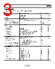
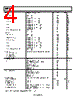
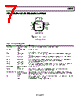
7 / 28 page  AD8366 Rev. A | Page 7 of 28 PIN CONFIGURATION AND FUNCTION DESCRIPTIONS PIN 1 INDICATOR 1 2 3 4 5 6 7 8 24 NOTES 1. THE EXPOSED PAD MUST BE CONNECTED TO GROUND. 23 22 21 20 19 18 17 VPSIA IPPA IPMA ENBL ICOM IPMB IPPB VPSIB BIT0/CS BIT1/SDAT BIT2/SCLK BIT3 OCOM BIT4 BIT5 DENA AD8366 TOP VIEW (Not to Scale) Figure 4. Pin Configuration Table 3. Pin Function Descriptions Pin No. Mnemonic Description 1, 8, 13, 28 VPSIA, VPSIB, VPSOB, VPSOA Input and Output Stage Positive Supply Voltage (4.75 V to 5.25 V). 2, 3, 6, 7 IPPA, IPMA, IPMB, IPPB Differential Inputs. 4 ENBL Chip Enable. Pull this pin high to enable. 5, 20 ICOM, OCOM Input and Output Ground Pins. Connect these pins via the lowest possible impedance to ground. 9, 32 DECB, DECA VPOS/2 Reference Decoupling Node. Connect a decoupling capacitor from these nodes to ground. 10, 31 OFSB, OFSA Output Offset Correction Loop Compensation. Connect a capacitor from these nodes to ground to enable the correction loop. Tie this pin to ground to disable. 11, 30 CCMB, CCMA Connect These Nodes to Ground. 12, 29 VCMB, VCMA Output Common-Mode Setpoint. These pins default to VPOS/2 if left open. Drive these pins from a low impedance source to change the output common-mode voltage. 14, 15, 26, 27 OPPB, OPMB, OPMA, OPPA Differential Outputs. 16, 17 DENB, DENA Data Enable. Pull these pins high to address each or both channels for parallel gain programming. These pins are not used in serial mode. 18, 19, 21, 22, 23, 24 BIT5, BIT4, BIT3, BIT2/SCLK, BIT1/SDAT, BIT0/CS Parallel Data Path (When SENB Is Low). When SENB is high, BIT0 becomes a chip select (CS), BIT1 becomes a serial data input (SDAT), and BIT2 becomes a serial clock (SCLK). BIT3 to BIT5 are not used in serial mode. 25 SENB Serial Interface Enable. Pull this pin high for serial gain programming mode and pull this pin low for parallel gain programming mode. EPAD The exposed pad must be connected to ground. |
|
|
链接网址 |
| ALLDATASHEET是否为您带来帮助? [ DONATE ] |
关于 Alldatasheet | 广告服务 | 联系我们 | 隐私政策 | 数据表链接 | 链接交换 | 制造商名单 All Rights Reserved©Alldatasheet.com |
| Russian : Alldatasheetru.com | Korean : Alldatasheet.co.kr | Spanish : Alldatasheet.es | French : Alldatasheet.fr | Italian : Alldatasheetit.com Portuguese : Alldatasheetpt.com | Polish : Alldatasheet.pl | Vietnamese : Alldatasheet.vn Indian : Alldatasheet.in | Mexican : Alldatasheet.com.mx | British : Alldatasheet.co.uk | New Zealand : Alldatasheet.co.nz |
|
Family Site : ic2ic.com |
icmetro.com |
 Chinese ▼
 English
 Chinese
 German
 Japanese
 Russian
 Korean
 Spanish
 French
 Italian
 Portuguese
 Polish
 Vietnamese
 Indian
 Mexican
 British
 New Zealand