|
数据搜索系统,热门电子元器件搜索 |
|
|
数据搜索系统,热门电子元器件搜索 |
|
AD8366ACPZ-R7 数据表(PDF) 26 Page - Analog Devices |
|
|
|||||||||||||||||||||||||||||
AD8366ACPZ-R7 数据表(HTML) 26 Page - Analog Devices |
|
|
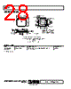
26 / 28 page  AD8366 Rev. A | Page 26 of 28 Figure 61. AD8366 Evaluation Board Printed Circuit Board (PCB), Top Side Figure 62. AD8366 Evaluation Board PCB, Bottom Side Table 5. Evaluation Board Configuration Options Components Function Default Conditions C1, C13 to C16, R3 to R6 Power supply decoupling. Nominal supply decoupling consists of a 0.1 μF capacitor to ground followed by 0.01 μF capacitors to ground positioned as close to the device as possible. C1 = 0.1 μF (size 0603), C13 to C16 = 0.01 μF (size 0402), R3 to R6 = 0 Ω (size 0603) T1, T2, C5, C18, C20, C21, R12 to R21, R44 to R48, R50, R54, R58, R62, R63 Input interface. The default configuration of the evaluation board is for single-ended operation. T1 and T2 are 4:1 impedance ratio baluns to transform a 50 Ω single-ended input into a 200 Ω balanced differential signal. R12 to R14 and R15, R16, and R19 are populated for appropriate balun interface. R44 to R48 and R50, R54, R58, R62, and R63 are provided for generic placement of matching components. C5, C18, C20, and C21 are balun decoupling capacitors. R17, R18, R20, and R21 can be populated with 0 Ω, and the balun interfacing resistors can be removed to bypass T1 and T2 for differential interfacing. T1, T2 = ADT4-6T+ (Mini-Circuits), C5, C20 = 0.1 μF (size 0402), C18, C21 = do not install, R12 to R16, R19, R44 to R47 = 0 Ω (size 0402), R17, R18, R20, R21,R48, R50, R54, R58, R62, and R63 = open (size 0402) T3, T4, C24 to C27, R29 to R31, R33 to R39, R65, R67 to R74, R80 Output interface. The default configuration of the evaluation board is for single-ended operation. T3 and T4 are 4:1 impedance ratio baluns to transform a 50 Ω single-ended output into a 200 Ω balanced differential load. R29 to R31, R33, R38, and R39 are populated for appropriate balun interface. R65, R67 to R74, and R80 are provided for generic placement of matching components. C24, C25, C26, and C27 are balun decoupling capacitors. R34 to R37 can be populated with 0 Ω, and the balun interfacing resistors can be removed to bypass T3 and T4 for differential interfacing. T3, T4 = ADT4-6T+ (Mini-Circuits), C24, C25 = 0.1 μF (size 0402), C26, C27 = do not install, R29 to R31, R33, R38, R39, R65, R67, R68, R80 = 0 Ω (size 0402), R34 to R37, R69 to R74 = open (size 0402) |
|
|
链接网址 |
| ALLDATASHEET是否为您带来帮助? [ DONATE ] |
关于 Alldatasheet | 广告服务 | 联系我们 | 隐私政策 | 数据表链接 | 链接交换 | 制造商名单 All Rights Reserved©Alldatasheet.com |
| Russian : Alldatasheetru.com | Korean : Alldatasheet.co.kr | Spanish : Alldatasheet.es | French : Alldatasheet.fr | Italian : Alldatasheetit.com Portuguese : Alldatasheetpt.com | Polish : Alldatasheet.pl | Vietnamese : Alldatasheet.vn Indian : Alldatasheet.in | Mexican : Alldatasheet.com.mx | British : Alldatasheet.co.uk | New Zealand : Alldatasheet.co.nz |
|
Family Site : ic2ic.com |
icmetro.com |
 Chinese ▼
 English
 Chinese
 German
 Japanese
 Russian
 Korean
 Spanish
 French
 Italian
 Portuguese
 Polish
 Vietnamese
 Indian
 Mexican
 British
 New Zealand