|
数据搜索系统,热门电子元器件搜索 |
|
|
数据搜索系统,热门电子元器件搜索 |
|
AD8366ACPZ-R7 数据表(PDF) 27 Page - Analog Devices |
|
|
|||||||||||||||||||||||||||||
AD8366ACPZ-R7 数据表(HTML) 27 Page - Analog Devices |
|
|
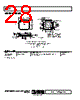
27 / 28 page  AD8366 Rev. A | Page 27 of 28 Components Function Default Conditions S1, S5, S7, R53, R57, R79, C29, C30, C31 Enable interface includes device enable and data enable. Device enable. The AD8366 is enabled by applying a logic high voltage to the ENBL pin. The device is enabled when the S1 switch is set in the down position (high), connecting the ENBL pin to VPSI_A. Data enable. DENA and DENB are used to enable the data path for Channel A and Channel B, respectively. Channel A is enabled when the S5 switch is set in the down position (high), connecting the DENA pin to VPSI_A. Likewise, Channel B is enabled when the S7 switch is set in the down position (high), connecting the DENB pin to VPSI_A. Both channels are disabled by setting the switches to the up position, connecting the DENA and DENB pins to GND. S1, S5, S7 = installed, R53, R57 = 5.1 kΩ (size 0603), R79 = 10 kΩ (size 0402), C30 = 0.01 μF (size 0402), C29, C31 = 1500 pF (size 0402) S2, S3, S4, S6, S8, S9, S10 R26, R32, R40 to R43, R61, R64, C23, C33, U1 Serial/parallel interface control. SENB is used to set the data control either in parallel or serial mode. The parallel interface is enabled when S4 is in the up position (low). The serial interface is enabled when S4 is in the down position (high). For SENB pulled low, BIT0 (S9) sets 0.25 dB gain, BIT1 (S2) sets 0.5 dB gain, BIT2 (S3) sets 1 dB gain, BIT3 (S6) sets 2 dB gain, BIT4 (S8) sets 4 dB gain, and BIT5 (S10) sets 8 dB gain. For SENB pulled high, BIT0 becomes a chip select (CS), BIT1 becomes a serial data input (SDAT), and BIT2 becomes serial clock (SCLK). BIT3 to BIT5 are not used in serial mode. U1 is used to deglitch the SCLK signal. S2, S3, S4, S6, S8, S9, S10 = installed, R26 = 698 kΩ (size 0603), R32, R40 to R43, R61, R64 = 5.1 kΩ (size 0603), C23, C33 = 1500 pF (size 0603), U1 = SN74LVC2G14 inverter chip S11, S12, C9, C10 DC offset correction loop compensation. The dc offset correction loop is enabled (high) with S11 and S12 for Channel A and Channel B, respectively, when the enabled pins, OFSA/ OFSB, are connected to ground through the C9 and C10 capacitors. When disabled (low), OFSA/OFSB are connected to ground directly. S11, S12 = installed, C9, C10 = 8200 pF (size 0402) R10, R22, R24, R28, C22, C28 Output common-mode setpoint. The output common mode on Channel A and Channel B can be set externally when applied to VCMA and VCMB. The resistive change through the potentiometer sets a variable VCMA voltage. If left open, the output common mode defaults to VPOS/2. R10, R24 = 10 kΩ potentiometers, R22, R28 = 0 Ω, C22, C28 = 0.1 μF (size 0402) C2, C3, C11, C12 Reference output decoupling capacitor to circuit common. C2, C3 = 0.1 μF (size 0402), C11, C12 = 0.01 μF (size 0402) |
|
|
链接网址 |
| ALLDATASHEET是否为您带来帮助? [ DONATE ] |
关于 Alldatasheet | 广告服务 | 联系我们 | 隐私政策 | 数据表链接 | 链接交换 | 制造商名单 All Rights Reserved©Alldatasheet.com |
| Russian : Alldatasheetru.com | Korean : Alldatasheet.co.kr | Spanish : Alldatasheet.es | French : Alldatasheet.fr | Italian : Alldatasheetit.com Portuguese : Alldatasheetpt.com | Polish : Alldatasheet.pl | Vietnamese : Alldatasheet.vn Indian : Alldatasheet.in | Mexican : Alldatasheet.com.mx | British : Alldatasheet.co.uk | New Zealand : Alldatasheet.co.nz |
|
Family Site : ic2ic.com |
icmetro.com |
 Chinese ▼
 English
 Chinese
 German
 Japanese
 Russian
 Korean
 Spanish
 French
 Italian
 Portuguese
 Polish
 Vietnamese
 Indian
 Mexican
 British
 New Zealand