|
数据搜索系统,热门电子元器件搜索 |
|
|
数据搜索系统,热门电子元器件搜索 |
|
AD8366ACPZ-R7 数据表(PDF) 16 Page - Analog Devices |
|
|
|||||||||||||||||||||||||||||
AD8366ACPZ-R7 数据表(HTML) 16 Page - Analog Devices |
|
|
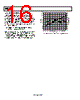
16 / 28 page  AD8366 Rev. A | Page 16 of 28 GAIN CONTROL INTERFACE The AD8366 provides two methods of digital gain control: serial or parallel. When the SENB pin is pulled low, the part is in parallel gain control mode. In this mode, the two digitally controlled VGAs can be programmed simultaneously, or one at a time, depending on the levels at DENA and DENB. If the SENB pin is pulled high, the part is in serial gain control mode, with Pin 24, Pin 23, and Pin 22 corresponding to the CS, SDAT, and SCLK signals, respectively. The voltage gain of the AD8366 is well approximated by Gain (dB) = GainCode × 0.253 + 4.5 Note that at several major transitions (15 to 16, 31 to 32, and 47 to 48), the gain changes significantly less (0 dB step) or significantly more (0.5 dB step) than the desired 0.25 dB step. This is inherent in the design of the part and is related to the partitioning of the variable gain block into a fine-gain and a coarse-gain section. –1.0 –0.8 –0.6 –0.4 –0.2 0 0.2 0.4 0.6 0.8 1.0 0 2.5 5.0 7.5 10.0 12.5 15.0 17.5 20.0 22.5 25.0 0 5 10 15 20 25 30 35 40 45 50 55 60 GAIN CODE Figure 49. Gain and Gain Step Error vs. Gain Code at 10 MHz |
|
|
链接网址 |
| ALLDATASHEET是否为您带来帮助? [ DONATE ] |
关于 Alldatasheet | 广告服务 | 联系我们 | 隐私政策 | 数据表链接 | 链接交换 | 制造商名单 All Rights Reserved©Alldatasheet.com |
| Russian : Alldatasheetru.com | Korean : Alldatasheet.co.kr | Spanish : Alldatasheet.es | French : Alldatasheet.fr | Italian : Alldatasheetit.com Portuguese : Alldatasheetpt.com | Polish : Alldatasheet.pl | Vietnamese : Alldatasheet.vn Indian : Alldatasheet.in | Mexican : Alldatasheet.com.mx | British : Alldatasheet.co.uk | New Zealand : Alldatasheet.co.nz |
|
Family Site : ic2ic.com |
icmetro.com |
 Chinese ▼
 English
 Chinese
 German
 Japanese
 Russian
 Korean
 Spanish
 French
 Italian
 Portuguese
 Polish
 Vietnamese
 Indian
 Mexican
 British
 New Zealand